Further, if
chemical reaction occurs between the wall material and reaction products, causing contaminants to deposit on the inner walls of the reaction chamber, the deposits that are gradually grown during long term use may fall off from the walls and enter the circuit formed on the wafer as
foreign matter, causing increase of percent defective of the products being processed.
However, if the region that generates the plasma is covered with
dielectric, the flow of charged particles dispersing from the plasma becomes unstable and the plasma potential is varied thereby, according to which stable processing becomes difficult.
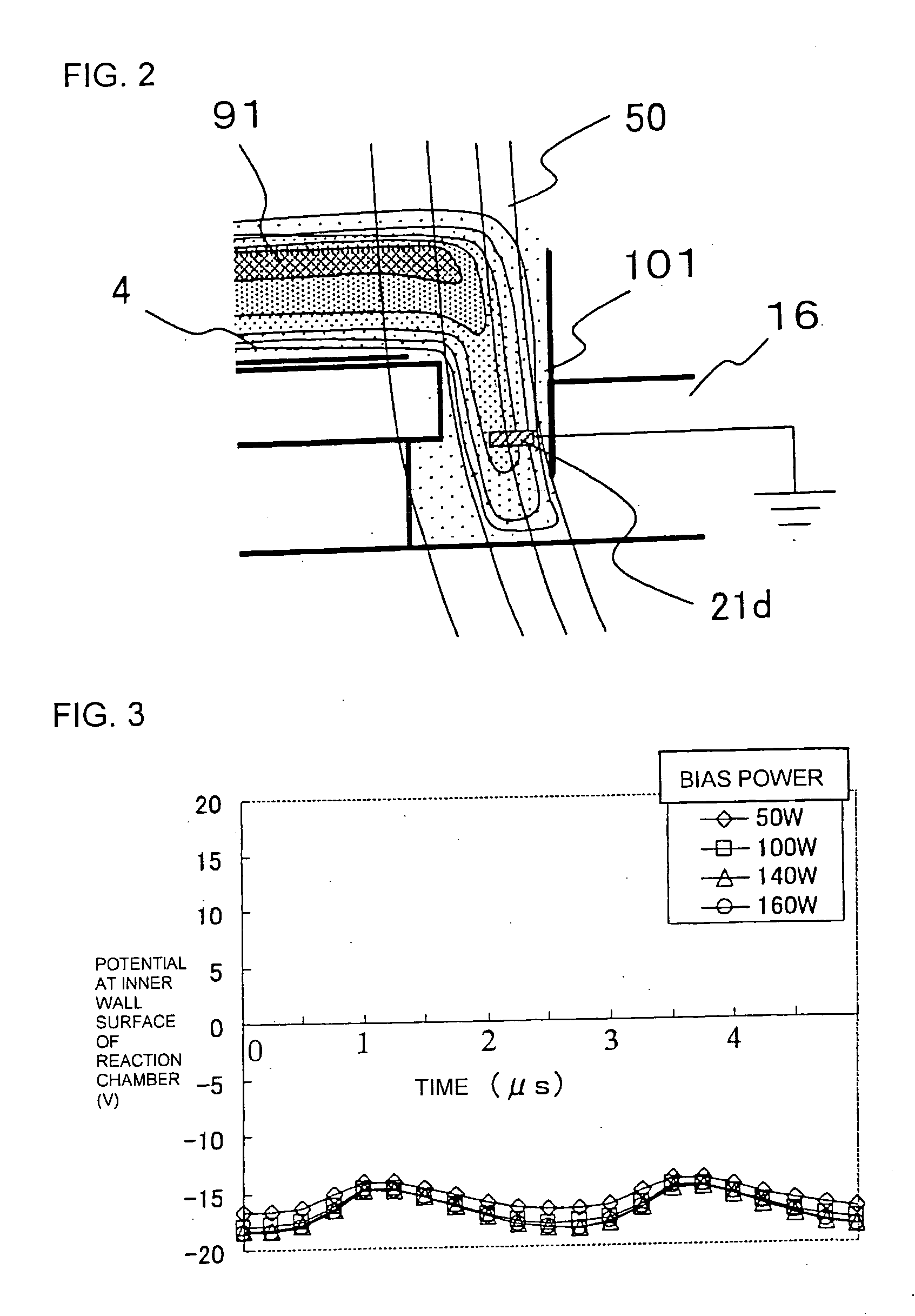
Further, the varying potential may cause damage to the wafers being processed. FIG. 6 shows the measured results of the potential waveforms at the inner wall surface of a
plasma etching apparatus having a reaction chamber formed of aluminum with the whole inner wall surface being anodized, wherein the measurement is performed using an
oscilloscope having its sensor mounted on the inner wall of the anodized aluminum reaction chamber.
This variation of potential at the inner wall surface is also caused according to various processing conditions, and especially, the DC-like potential variation has no reproducibility and shows unstable behavior according to some
discharge conditions.
Further, if such potential variation of plasma occurs, an
electric field is induced within the processed wafer surface, causing electrical damage to the circuit formed on the wafer and resulting in deterioration of
product property and increase of defective fraction.
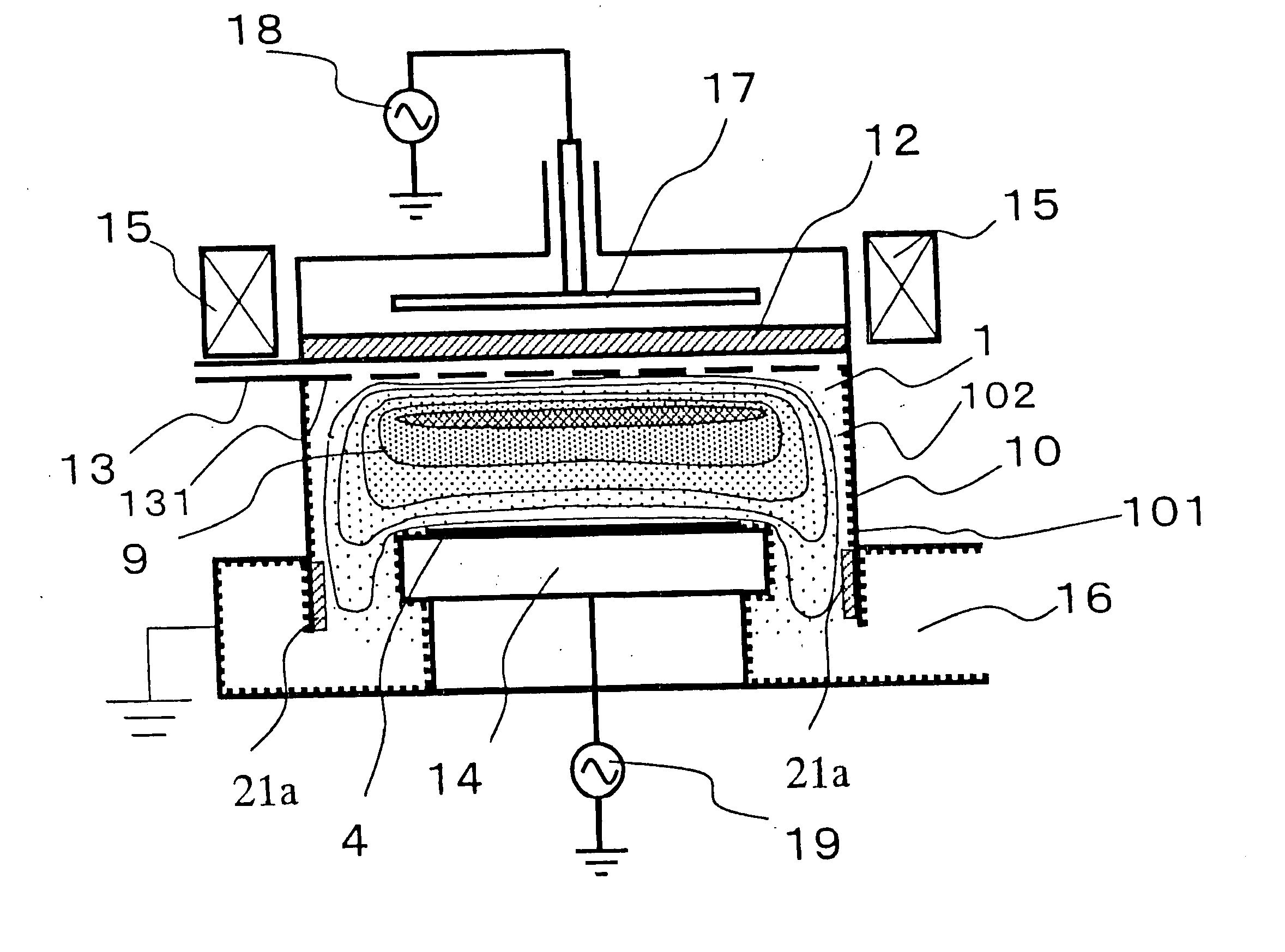
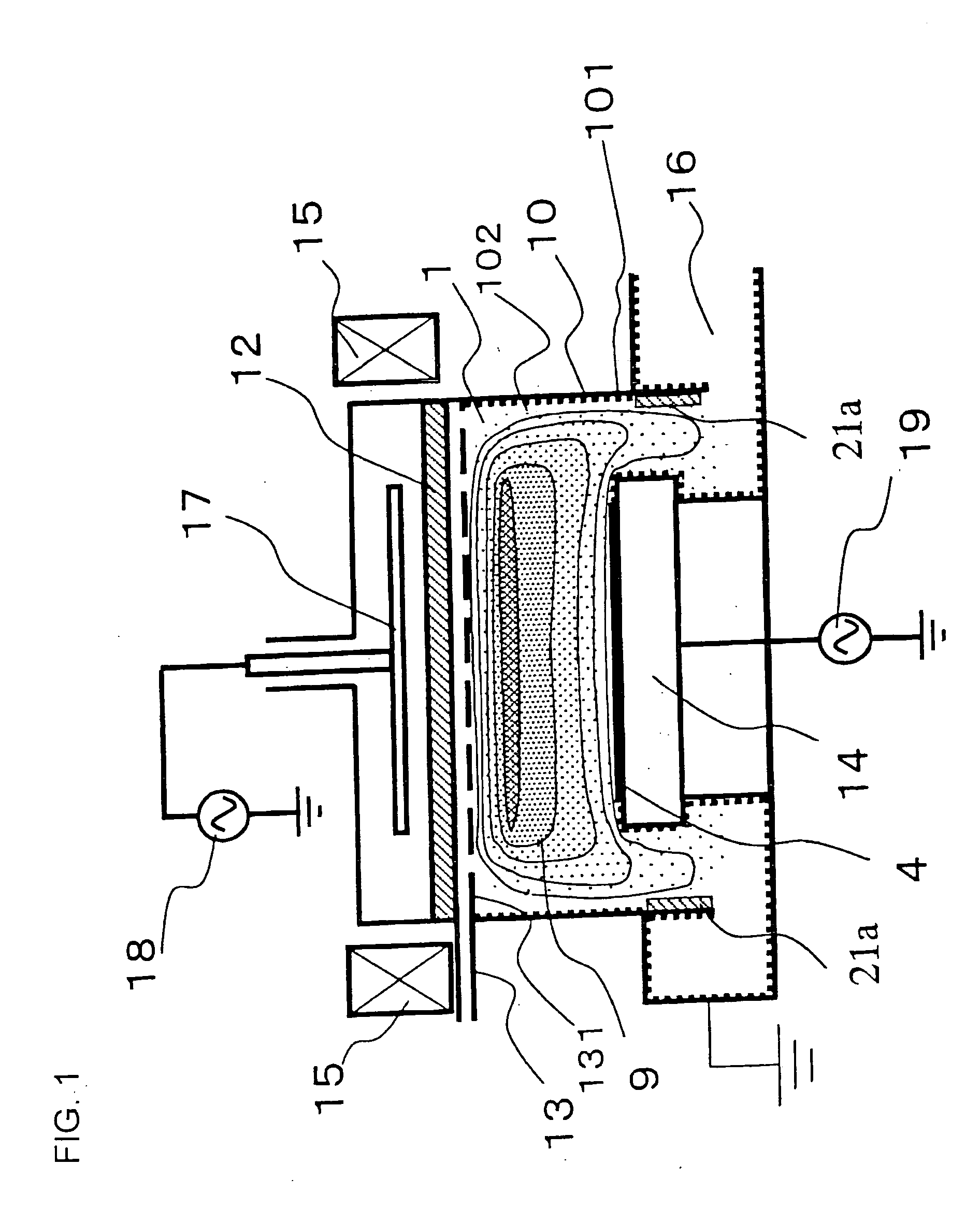
In an
inductively coupled plasma etching apparatus, there is no
electrode serving as a potential reference within the reaction chamber since an
induction coil disposed outside the
dielectric vacuum window is used to apply high frequency and generate plasma in the chamber, so the plasma potential tends to be varied, causing damage to the circuit formed on the wafer.
According to this method, however, the DC-like potential variation is not necessarily stabilized, and if an insulative protective
coating is formed on the earth point surface, the DC-like potential variation as shown in FIG. 6 cannot be reduced.
Therefore, this prior art disclosure only mentions the effect of suppressing the variation in processing conditions caused by the alumite being chipped away, and does not consider suppressing the potential variation of plasma or reducing the damage of the earth.
However, if the inner surface of the reaction chamber is covered with insulating protective
coating, the plasma becomes unstable, causing damage to the LSI circuits or deteriorating the long-term stability of the process.
In order to solve such problems, an earth point was provided in the processing chamber as disclosed in above-mentioned
Patent Document 1, but by simply providing an earth point, only the potential variation of plasma was stabilized, and the problem of the reaction chamber being damaged by the
ion sputtering caused by the high frequency applied to the wafer could not be solved.
That is, if the earth point is located at the corner of the
plasma reaction chamber, the
plasma density coming into contact therewith falls and the electric resistance between the plasma near the earth and the earth point becomes large, between which occurs the fall of potential, and the function as earth
electrode is deteriorated.
Moreover, if a protective
coating formed of an insulating material is provided on the earth point surface, the plasma potential cannot be stabilized with respect to DC-like or low-frequency potential variations.
Furthermore, the disclosure related to providing the earth point does not consider the effect of reducing the damage to the inner wall of the reaction chamber or to the earth caused by the high frequencies applied to the wafer by providing the earth point.
Furthermore, the reactive gas used in the
etching process comes into direct contact with the base material, causing the material to be damaged by
chemical reaction and increasing the amount of
metal impurities entering the wafer.

