RFID tag

Inactive Publication Date: 2009-04-09
HITACHI LTD
View PDF6 Cites 5 Cited by
  • Summary
  • Abstract
  • Description
  • Claims
  • Application Information

AI Technical Summary

Benefits of technology

[0026]According to the present invention, it is possible to suppress variations in the capacity component that occur at the time of physical

Problems solved by technology

Since electromagnetic waves are damped in proportion to the square to cube of their travel distance, if the travel distance increases, electromagnetic waves having been radiated from a base station experience a drastic power loss by the time they arrive at the base station again, and exhibit very low resistance due to a number of diverse disturbance factors.

Method used


Image

  • RFID tag
  • RFID tag
  • RFID tag

Examples


embodiment 1

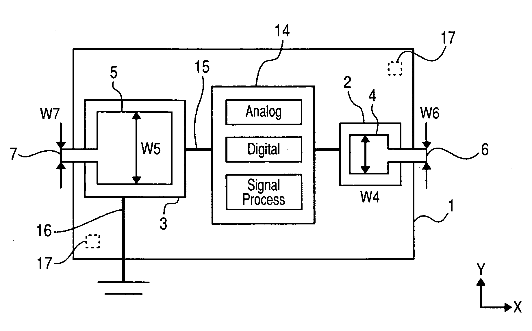
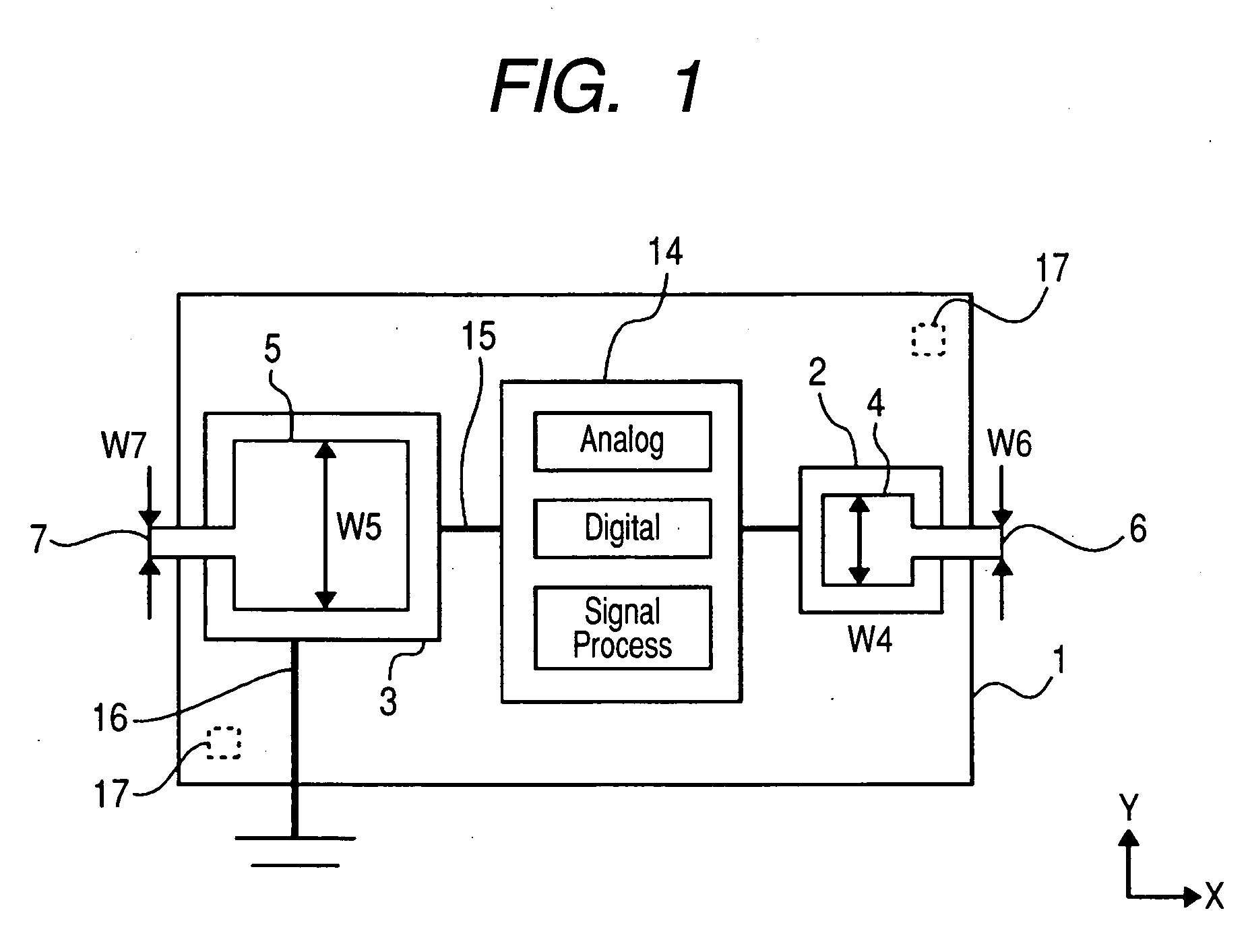
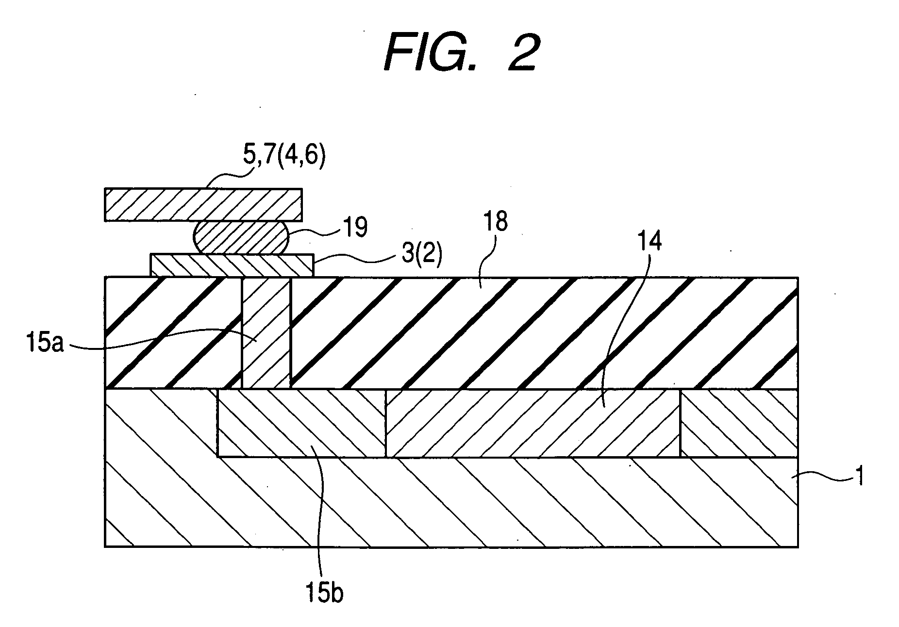
[0058]With reference to FIG. 1 through FIG. 4, the following will now explain one embodiment of the present invention. FIG. 1 is a plan view showing a configuration example for an RFID tag in accordance with one embodiment of the present invention. On a rectangular semiconductor chip (RFID chip) 1, an electrode 2 for hot contact that is not connected to the earth potential of a semiconductor chip, an electrode 3 for earth contact that is connected to the earth potential of the semiconductor chip, an electrode 4 for hot contact of an antenna, an electrode 5 for earth contact of the antenna, a hot draw-out conductor 6 of the antenna, and an earth draw-out conductor 7 of the antenna are formed. The planar shape of each of the electric contacts 4 and 5 of the external antenna is encompassed by the planar shape of each of the electric contacts 2 and 3 of the semiconductor chip. That is to say, the size of the rectangular electric contact 4 is smaller than the plane of the rectangular ele...

embodiment 2

[0069]Another embodiment of the present invention will now be explained with reference to FIG. 6. FIG. 6 is a plan view showing the configuration of an RFID tag in accordance with another embodiment of the present invention. The RFID tag of this embodiment differs from the embodiment of FIG. 1 in that connecting conductors are all circular. That is, an electrode 52 for hot contact that is not connected to the earth potential of a semiconductor chip, an earth contact electrode 53 that is connected to the earth potential of the semiconductor chip, an electrode 54 for hot contact of an antenna, and an earth contact electrode 55 of the antenna all have a circular-planar shape. The width W7 of an earth draw-out conductor 7 of the antenna in the Y direction is smaller than the size (diameter D5 of circle) of an electric contact 5. Similarly, the width of a hot draw-out conductor 6 of the antenna in the Y direction is smaller than the size of an electric contact 4.

[0070]In addition to the ...

embodiment 3

[0071]Yet another embodiment of the present invention will now be explained with reference to FIG. 7. FIG. 7 is a plan view showing the configuration of an RFID tag in accordance with yet another embodiment of the present invention. The RFID tag of this embodiment differs from the embodiment of FIG. 1 in that all connecting conductors have a hexagonal shape, one of polygons. That is, an electrode 62 for hot contact that is not connected to the earth potential of a semiconductor chip, an earth contact electrode 63 that is connected to the earth potential of the semiconductor chip, an electrode 64 for hot contact of an antenna, and an earth contact electrode 65 of the antenna all have a hexagonal-planar shape. The width of a hot draw-out conductor 64 of the antenna in the Y direction is smaller than the size (width in X and Y directions) of the electric contact 62. Similarly, the width of earth draw-out electrode 65 of the antenna is smaller than the size of the electric contact 63.

[0...


PUM


Abstract

An RFID tag of the present invention is provided to suppress variations in the capacity component that occur during physical coupling between an antenna and a semiconductor chip as part of the manufacturing process. The RFID tag includes an antenna with a pair of electric contacts, draw-out conductors of the electric contacts, and an RFID chip with a pair of electric contacts, wherein the electric contacts of the antenna are encompassed to their corresponding electric contacts of the RFID chip, and draw-out electrodes are drawn out in an opposite direction to the facing direction overlapped direction).

Description

CLAIM OF PRIORITY[0001]The present application claims priority from Japanese Patent Application 2007-262290 filed on Oct. 5, 2007, the content of which is hereby incorporated by reference into this application.FIELD OF THE INVENTION[0002]The present invention relates to an RFID tag, more specifically, to the construction of a mobile terminal used for a wireless RF-ID communication system, in which electromagnetic waves that are radiated by a base station are scattered by an unspecified object or a mobile terminal, and arrive at the base station again, while the base station receives the incoming electromagnetic waves and identifies the object—or the mobile terminal-specific information.BACKGROUND OF THE INVENTION[0003]One of well-known conventional techniques is a direction division duplex (DDD) scheme implemented in systems where scattered waves are used directly as carrier waves. In this technique, a circulator is used to carry out equivalent duplexing of a transmitting wave and a...

Claims


Application Information

Patent Timeline
IPC IPC(8): G08B13/14
CPCG06K19/0775H01Q21/28H01Q9/0407H01Q1/2225
Inventor TAKEI, KEN
Owner HITACHI LTD
Why Eureka
Try Eureka