

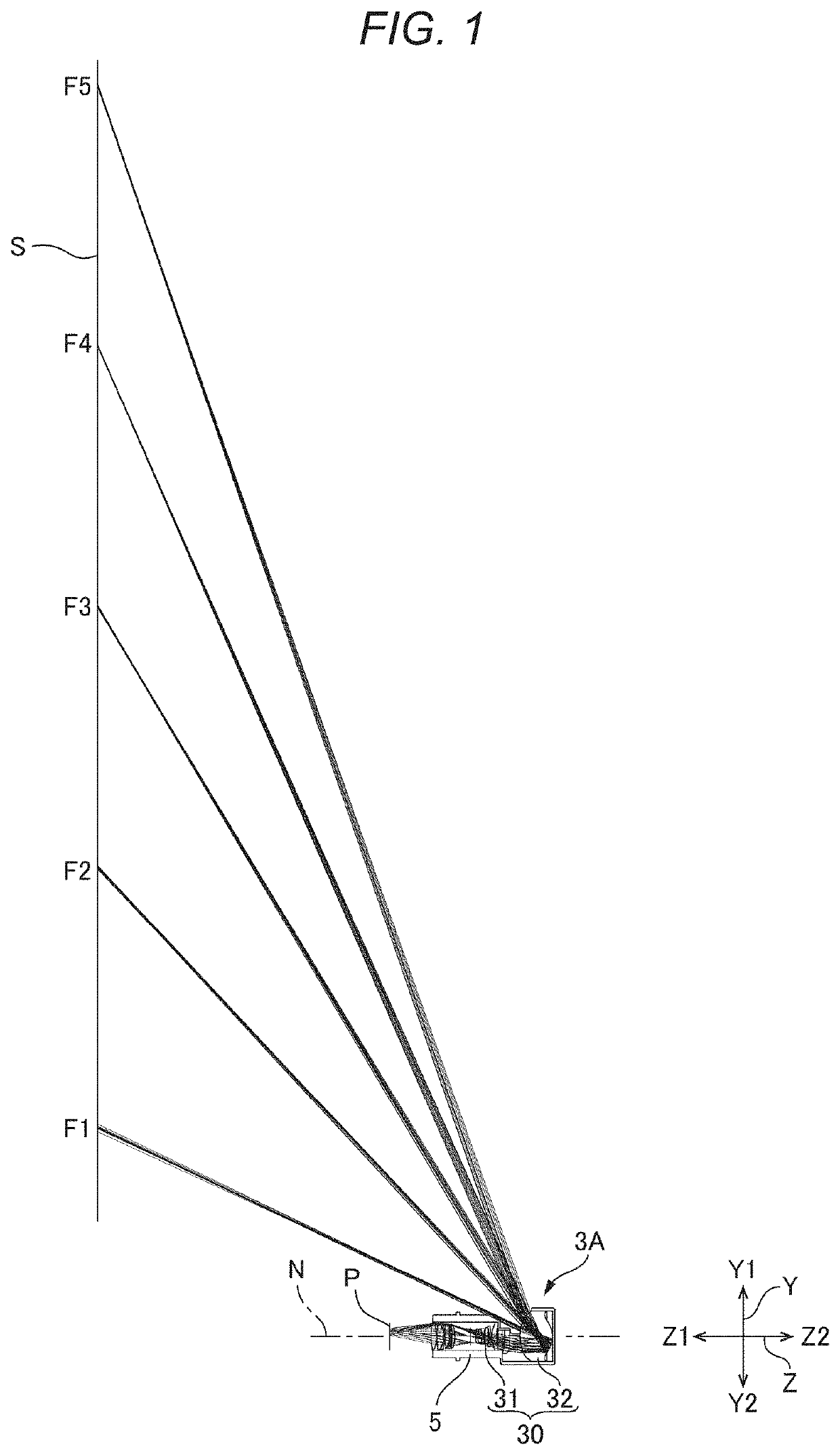
Optical device, projector, and imaging device
a technology of optical devices and imaging devices, applied in the field of optical devices, projectors, imaging devices, can solve the problems of not being able to cover the exit surface of the lens, and achieve the effect of preventing or suppressing, and preventing deterioration of image quality
- Summary
- Abstract
- Description
- Claims
- Application Information
AI Technical Summary
Benefits of technology
Problems solved by technology
Method used
Image

Examples
modified examples
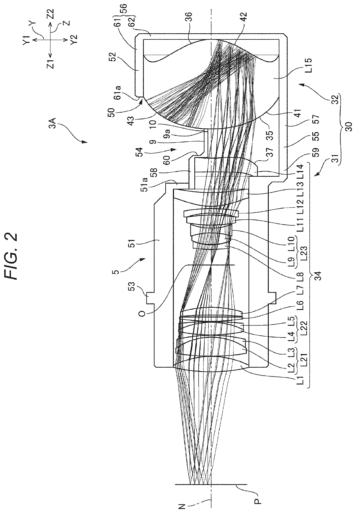
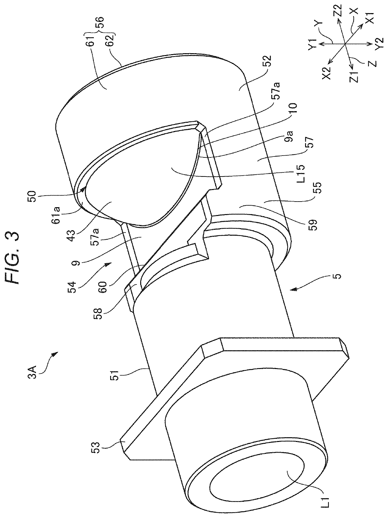
[0041]FIG. 4 is an explanatory diagram of the optical device 3A according to Modified Example 1. FIG. 5 is an explanatory diagram of the optical device 3A according to Modified Example 2. The optical device 3A according to Modified Example 1 and the optical device 3A according to Modified Example 2 are different in configuration of the optical device 3A and the partition wall 9 from each other, but are the same in other configurations as each other. Therefore, in the description of the optical device 3A according to Modified Example 1 and the optical device 3A according co Modified Example 2, the configurations corresponding to those of the optical device described above are denoted by the same reference symbols, and the description thereof will be omitted.
[0042]As shown in FIG. 4, in the optical device 3A according to Modified Example 1, the partition wall 9 is disposed on the first surface 35 of the lens L15. More specifically, the partition wall 9 has a plate-like shape, and prot...
example 3
Practical Example 3
[0059]FIG. 9 is a ray chart of an optical device 3C according to Practical Example 3. It should be noted that the optical device 3C according to the present example is provided with constituents corresponding to those of the optical device 3A described above. Therefore, the corresponding constituents are denoted by the same reference symbols, and the description thereof will be omitted. As shown in FIG. 9, the optical device 3C according to the present example is provided with the first optical system 31 and the second optical system 32 in this order from the reduction side toward the enlargement side. Further, the optical device 3C is provided with the holding member 5 for holding the first optical system 31 and the second optical system 32, and the partition wall 9.
[0060]The first optical system 31 is provided with a lens L36 and the lens L37 (the second optical element). The lens L36 and the lens L37 are arranged in a direction crossing the optical axis N betwe...
PUM
| Property | Measurement | Unit |
|---|---|---|
| surface shape | aaaaa | aaaaa |
| height | aaaaa | aaaaa |
| convex shape | aaaaa | aaaaa |
Abstract
Description
Claims
Application Information