Method for forming film by using atomic layer deposition method

A technique of atomic layer deposition and atomic layer, which is applied in chemical instruments and methods, coatings, metal material coating processes, etc., can solve the problems of damaging the properties of insulating films and not being able to obtain thin film properties, etc.

Inactive Publication Date: 2006-01-04
SAMSUNG ELECTRONICS CO LTD
View PDF0 Cites 0 Cited by
  • Summary
  • Abstract
  • Description
  • Claims
  • Application Information

AI Technical Summary

Problems solved by technology

When containing such as Al(OH) 3 When impurities are present, the desired film properties cannot be obtained
In particular, when containing Al(OH) 3 When an aluminum oxide film is used as an insulating film for a semiconductor device, this Al(OH) 3 The aluminum oxide film will act as an electron trap or leakage point, thereby damaging the characteristics of the insulating film

Method used


Image

  • Method for forming film by using atomic layer deposition method
  • Method for forming film by using atomic layer deposition method
  • Method for forming film by using atomic layer deposition method

Examples


no. 1 example

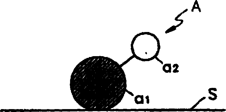
[0058] Figure 4A to Figure 4D The reaction mechanism of the method of forming a thin film using the ALD method according to the first embodiment of the present invention is shown. By injecting the first reactant A into the reaction chamber 11 equipped with the substrate, the first reactant is chemisorbed into the substrate 15 such as the silicon substrate, wherein the first reactant consists of the atoms a forming the film 1 and ligand a 2 After the first reactant A is adsorbed into the substrate 15, the first reactant A physically adsorbed is removed by injecting an inert gas to purge the reaction chamber ( Figure 4A ).

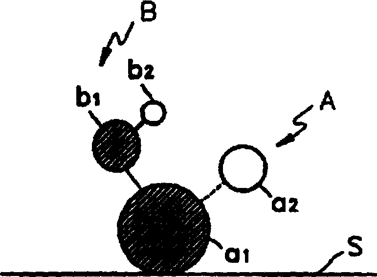
[0059] The second reactant B is injected into the reaction chamber 11 containing the substrate where the first reactant A has been adsorbed. Thus, the second reactant B is chemisorbed into the first reactant A. An imperfect material that actively reacts with the first reactant A is used as the second reactant B. A substance is used as the second react...

no. 2 example

[0095] Figure 22 A flowchart showing a second embodiment of the method of forming a thin film using the ALD method according to the present invention. Rinse the substrate with oxygen ( image 3 In 15), for example, a silicon substrate using an oxidizing gas, the dangling bonds of the substrate 15 are combined with oxygen to perform a termination treatment (step 21). That is, at any point where oxygen can bind to the substrate 15, by flushing the substrate with oxygen ( image 3 In 15) oxygen is bound to the substrate, for example flushing the silicon substrate with an oxidizing gas.

[0096] The dangling bonds can be combined with oxygen, that is, not only by oxygen rinsing, but also by ozone rinsing and by forming a silicon oxide film so that oxygen is bound to any available site on the substrate. In addition, no oxygen flushing may be performed on the substrate 15 .

[0097] Substrate 15 is loaded into reaction chamber ( image 3 In 11) after, utilize heater (not shown...

no. 3 example

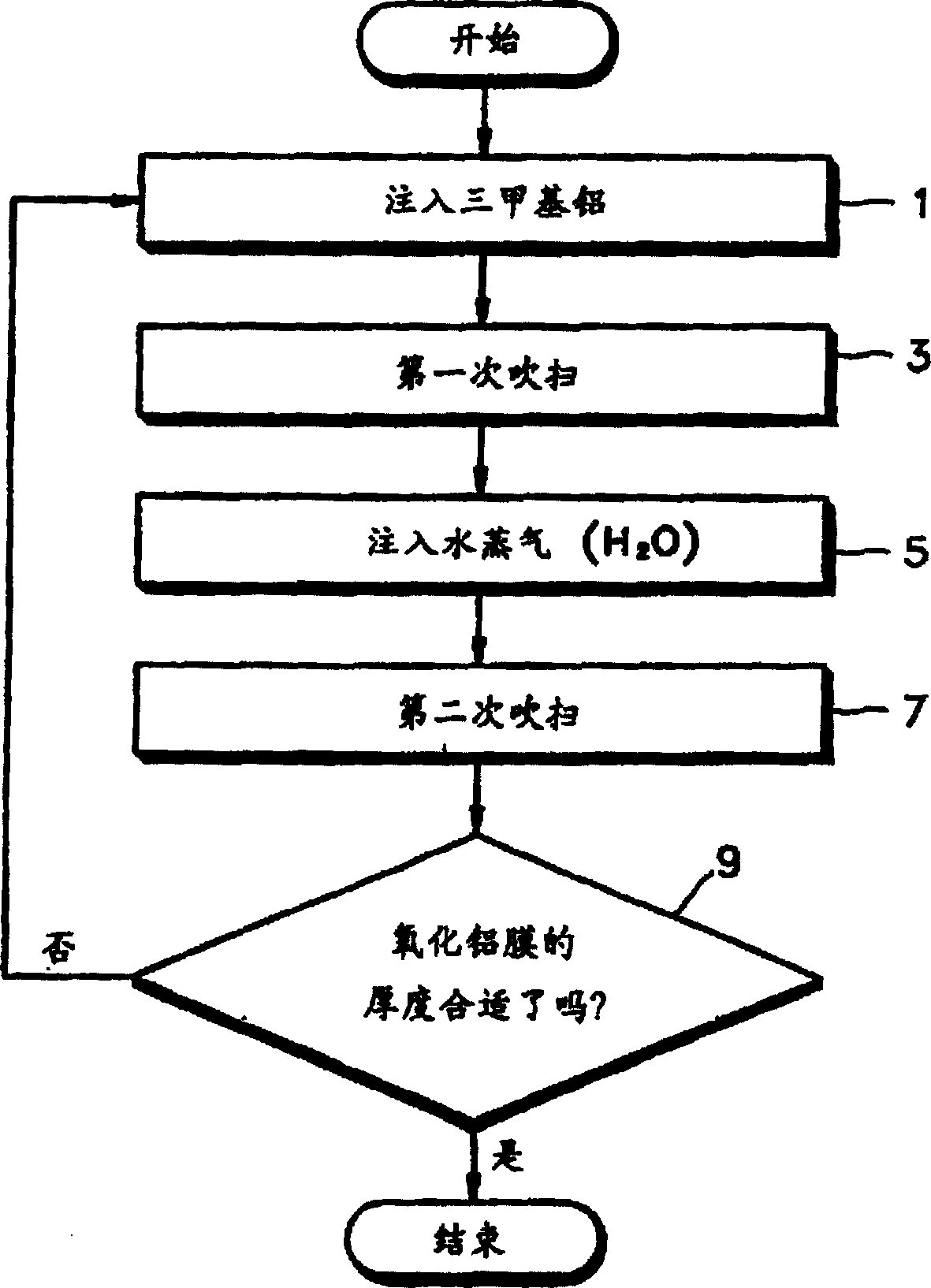
[0119] Figure 26 A flowchart showing a method of forming a thin film by the ALD method according to the third embodiment of the present invention. Figure 27 is a timing chart showing the supply of reactants during thin film formation by the ALD method of the third embodiment of the present invention. In the following description, the formation of an aluminum oxide film is taken as an example.

[0120] Oxygen cleaning or nitrogen cleaning is performed on the substrate 15 with an oxidizing gas or a nitriding gas, so that the dangling bonds of the substrate are terminated, and the substrate may be a silicon substrate (step 41 ). That is, at any point where oxygen can bind to the substrate, the substrate can be a silicon substrate, by using an oxidizing gas or a nitriding gas to bind oxygen to the substrate by oxygen flushing or nitrogen flushing. Not only can use image 3 The atomic layer thin film forming apparatus is shown, and other apparatuses may be used for oxygen flus...


PUM

PropertyMeasurementUnit
thicknessaaaaaaaaaa

Abstract

In a method of forming a thin film using an atomic layer deposition (ALD) method, a thin film is formed on a substrate in cycles. Each cycle includes injecting a first reactant including an atom that forms the thin film and a ligand into a reaction chamber that includes the substrate, purging the first reactant, injecting a second reactant into the reaction chamber, and purging the second reactant. The thin film is formed by a chemical reaction between the atom that forms the thin film and a second reactant whose binding energy with respect to the atom that forms the thin film is larger than the binding energy of the ligand with respect to the atom that forms the thin film and the generation of by-products is prevented. The generation of a hydroxide by-product in the thin film is suppressed by using a material that does not include a hydroxide as the second reactant, purging the second reactant, and reacting the second reactant with a third reactant that includes hydroxide. After purging the second reactant, the third reactant for removing impurities and improving the stoichiometry of the thin film is injected and purged. In this way, it is possible to obtain a thin film that does not include impurities and whose stoichiometry is excellent.

Description

technical field [0001] The invention relates to a method for forming a thin film, in particular to a method for forming a thin film by atomic layer deposition (ALD). Background technique [0002] Generally, thin films are used as insulating materials for semiconductor devices, transparent conductors for liquid crystal displays, and protective layers for electroluminescent thin film displays. The thin film can be formed by a solution-gel method, a sputtering method, a plating method, an evaporation method, a chemical vapor deposition (CVD) method, or an ALD method. [0003] Among these methods, the ALD method is likely to obtain better step coverage than the CVD method, and low-temperature processing is possible with the ALD method. In the ALD method, a thin film is formed by decomposing a reactant, not by pyrolysis, but by periodically supplying each reactant for chemical exchange. Here, a method of forming an aluminum oxide film that can be used as an insulating film of a...

Claims


Application Information

Patent Timeline
Patent Type & Authority Patents(China)
IPC IPC(8): C23C26/00C23C16/40C23C16/34C23C16/44C30B25/02H01L21/314H01L21/316H01L21/318
CPCC23C16/403C23C16/45525H01L21/31691H01L21/316C30B25/02C23C16/409C30B29/20H01L21/02164H01L21/02183H01L21/02189H01L21/02192H01L21/02178H01L21/02181H01L21/0228H01L21/02186H01L21/02197
Inventor 金荣宽朴泳旭林载顺崔城济李相忍
Owner SAMSUNG ELECTRONICS CO LTD
Why Eureka
Try Eureka