Multiple charged particle beam writing apparatus and multiple charged particle beam writing method
- Summary
- Abstract
- Description
- Claims
- Application Information
AI Technical Summary
Problems solved by technology
Method used
Image

Examples
Example
First Embodiment
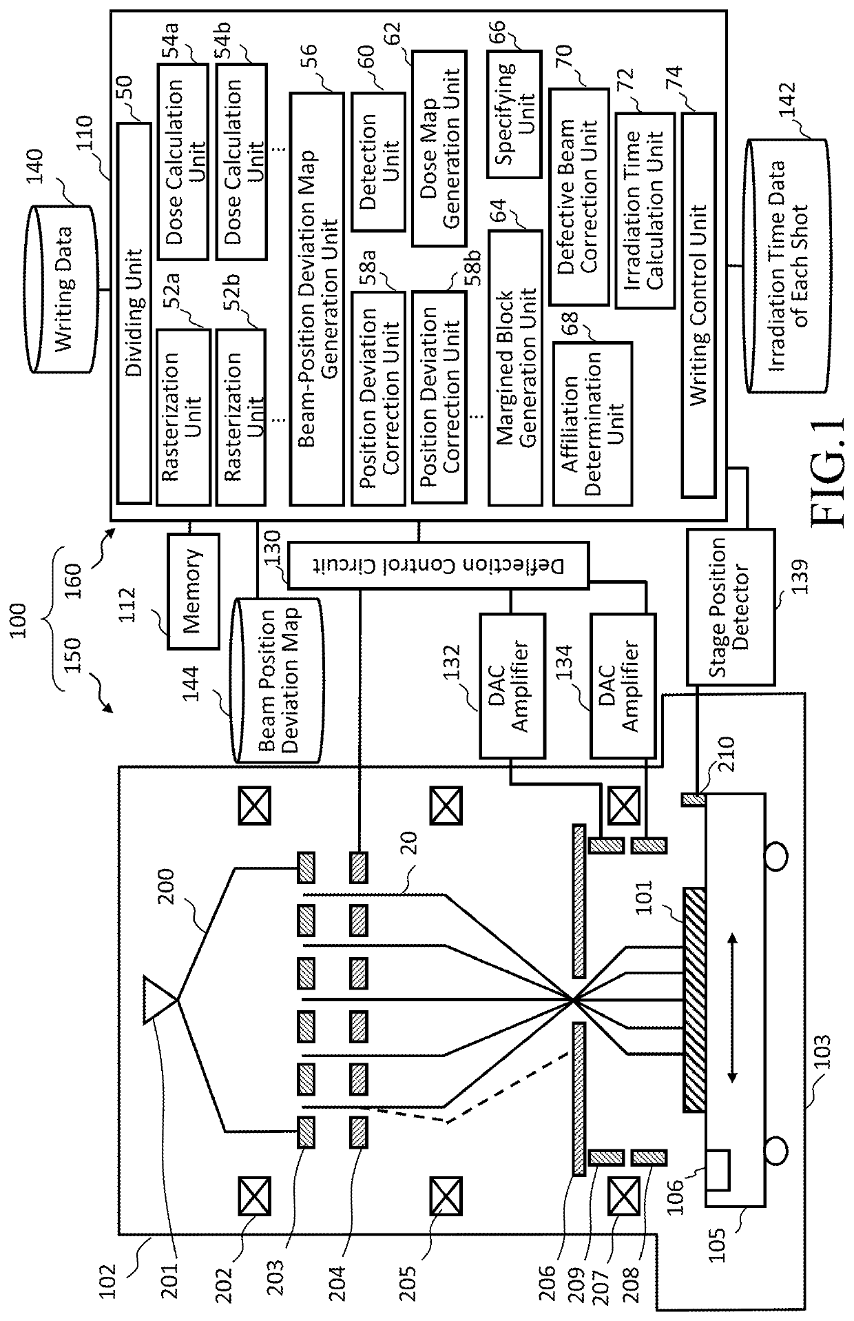
[0057]FIG. 1 is a schematic diagram showing a configuration of a writing or “drawing” apparatus according to a first embodiment. As shown in FIG. 1, a writing apparatus 100 includes a writing mechanism 150 and a control system circuit160. The writing apparatus 100 is an example of a multiple charged particle beam writing apparatus. The writing mechanism 150 includes an electron beam column 102 (multiple electron beam column) and a writing chamber 103. In the electron beam column 102, there are disposed an electron gun 201, an illumination lens 202, a shaping aperture array substrate 203, a blanking aperture array mechanism 204, a reducing lens 205, a limiting aperture substrate 206, an objective lens 207, a deflector 208, and a deflector 209. In the writing chamber 103, an XY stage 105 is disposed. On the XY stage 105, there is placed a target object or “sample”101 such as a mask blank on which resist has been applied serving as a writing target substrate when writin...
Example
Second Embodiment
[0124]Although the first embodiment describes a configuration in which affiliation of the pixel irradiated with a defective beam is determined using a dose map of before correcting position deviation, it is not limited thereto. A second embodiment describes a configuration in which affiliation of the pixel irradiated with a defective beam is determined using a dose map of after correcting position deviation. The configuration of the writing apparatus 100 in the second embodiment is the same as that of FIG. 1. Further, the contents of the second embodiment are the same as those of the first embodiment except for what is particularly described below.
[0125]FIG. 15 is a flowchart showing main steps of a writing method according to the second embodiment. The contents shown in FIG. 15 are the same as those in FIG. 7 except for the arrow indicating that the dose map used for the defective beam affiliation determining step (S120) is a position deviation correction dose map....
Example
Third Embodiment
[0130]Although the first and second embodiments describe a configuration in which a defective beam is corrected after affiliating each pixel irradiated with a defective beam to a corresponding margined block region 33, it is not limited thereto. A third embodiment describes a configuration in which defective beam correction may be redundantly performed.
[0131]FIG. 16 is a conceptual diagram showing a configuration of a writing apparatus according to the third embodiment. FIG. 16 is the same as FIG. 1 except for that a data processing unit 71 and a plurality of defective beam correction units 76 (76a, 76b, . . . ), are disposed in the control computer 110, instead of the affiliation determination unit 68 and the defective beam correction unit 70. Each of the “units” such as the dividing unit 50, the plurality of rasterization units 52 (52a, 52b, . . . ), the plurality of dose calculation units 54 (54a, 54b, . . . ), the beam-position deviation map generation unit 56, t...
PUM
 Abstract
Description
Claims
Application Information
 - R&D Engineer
- R&D Manager
- IP Professional
- Industry Leading Data Capabilities
- Powerful AI technology
- Patent DNA Extraction
Browse by: Latest US Patents, China's latest patents, Technical Efficacy Thesaurus, Application Domain, Technology Topic.
© 2024 PatSnap. All rights reserved.Legal|Privacy policy|Modern Slavery Act Transparency Statement|Sitemap