Touch display device

Active Publication Date: 2022-04-28
WUHAN CHINA STAR OPTOELECTRONICS SEMICON DISPLAY TECH CO LTD
View PDF0 Cites 0 Cited by
  • Summary
  • Abstract
  • Description
  • Claims
  • Application Information

AI Technical Summary

Benefits of technology

The present invention is a touch display device that uses a touch layer to replace both a capacitor touch unit and a pressure touch unit. This allows for two-dimensional and three-dimensional inspections of the touch display device. The touch layer is easy to use, lightweight, and compact, without adding difficulty to the wiring process, and also reduces the manufacturing costs.

Problems solved by technology

At present, most of touch display panels can only implement two dimensional (2D) coordinate inspection and cannot perform three dimensional (3D) coordinate inspection.
In the prior art, to achieve three dimensional (3D) coordinate inspection, a user employs opposite independent capacitor touch unit and a pressure touch unit, which makes the structural design of the display device complicated and increases the cost of the touch display device.

Method used


Image

  • Touch display device
  • Touch display device
  • Touch display device

Examples


first embodiment

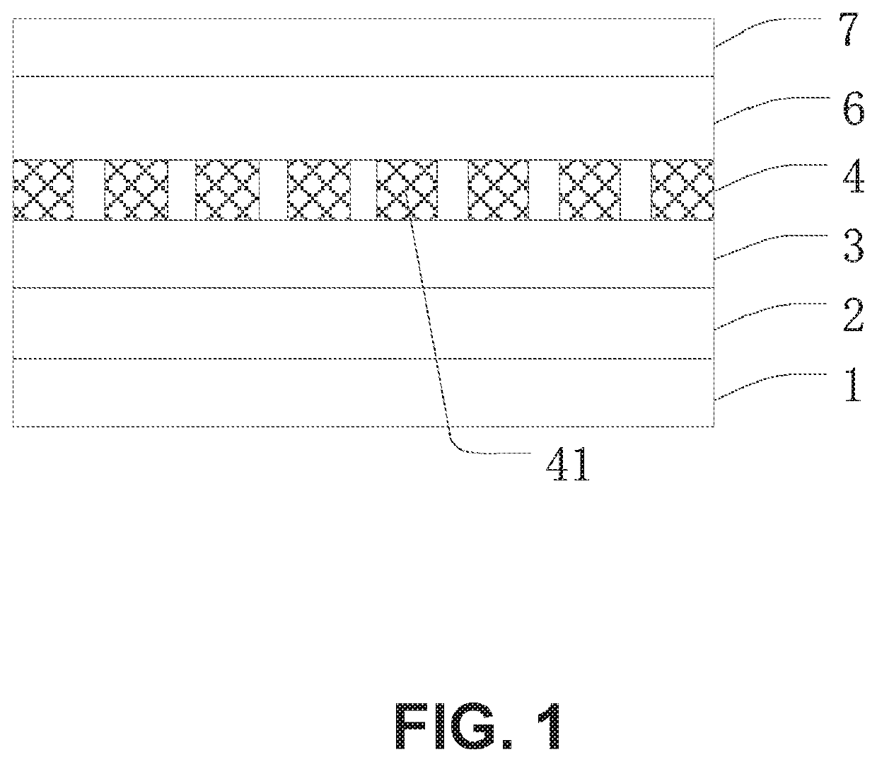
[0033]The embodiment of the present invention provides a touch display device, the touch display device in an aspect can achieve display functions and in another aspect can allow users to implement touch operation, which further achieve corresponding control.

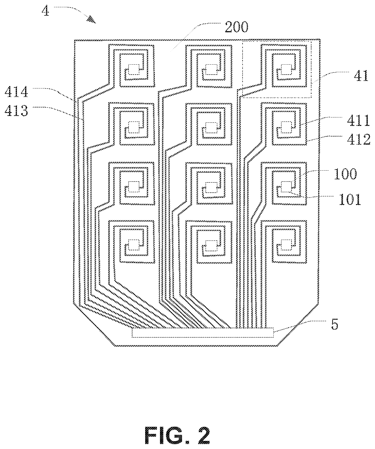
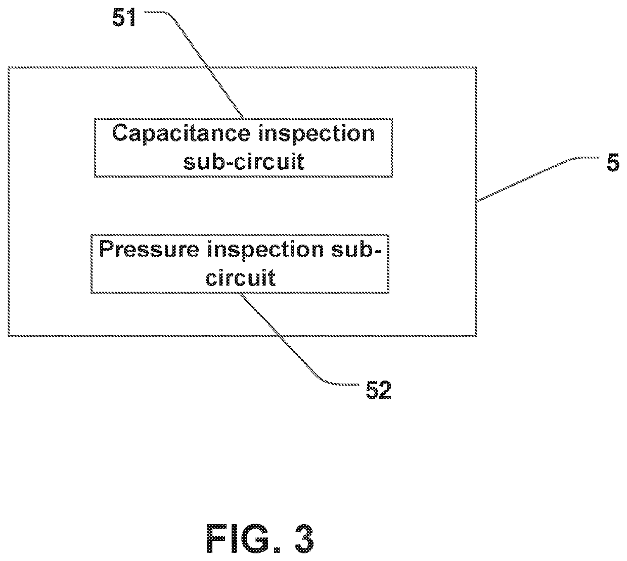
[0034]With reference to FIGS. 1 to 2, the touch display device comprises a substrate 1, a light emitting layer 2, an encapsulation layer 3, a touch layer 4, a touch driver inspection circuit 5, an optical clear adhesive layer 6, and a cover plate 7.

[0035]The substrate 1 is an array substrate and comprises a plurality of thin film transistor configured to drive the touch display device to operate.

[0036]The light emitting layer 2 is disposed on the substrate, and the light emitting layer 2 is preferably an organic light emitting diode (OLED) light emitting layer. Driven by an electrical field, an organic semiconductor material and a light emitting material emit light by carrier injecotion and compounding.

[0037]The encapsulation la...

second embodiment

[0054]The embodiment of the present invention provides a touch display device comprising most of the technical solutions in the first embodiment 1. A different thereof is that the touch display device further comprises a first insulation layer 9, a first through hole 10, a second insulation layer 11, and a second through hole 12.

[0055]With reference to FIG. 6, a first insulation layer 9 is disposed between the first lead wire 413 and the touch electrode units 41. The first lead wire 413 is electrically connected to another end of the first touch electrode wire 411 through the first through hole 10 defined in the first insulation layer such that the first lead wire 413 and the first touch electrode wire 411 are disposed in different layers to reduce a distance between adjacent two of the touch electrode units 41. In other words, a space of the blind region 200 is reduced to further improve the touch sensitivity of the touch display device and optimize the touch capability.

[0056]With ...


PUM


Abstract

A touch display device is provided and includes a substrate, light emitting layer, encapsulation layer, a touch layer, and a touch driver inspection circuit. The touch layer includes a plurality of touch electrode units. The touch driver inspection circuit is connected to each of the touch electrode units the touch layer and is configured to monitor a touch position according to variation of a capacitance of the touch electrode units. The touch driver inspection circuit is further configured to monitor a pressure of the touch position according to variation of pressures on the touch electrode units.

Description

FIELD OF INVENTION[0001]The present invention relates to a field of displays, especially relates to a touch display device.BACKGROUND OF INVENTION[0002]For a touch display device, touch operation is an important human-computer interaction operation. Therefore, precisely inspecting parameters of touch operation is one important means for guaranteeing user experience of the touch display device.[0003]A touch display device comprises a touch display panel. At present, most of touch display panels can only implement two dimensional (2D) coordinate inspection and cannot perform three dimensional (3D) coordinate inspection. The 2D coordinate inspection can inspect a coordinate of a touch position of a finger on a surface of the touch display panel along a X-axis direction and a Y-axis direction. The 3D coordinate inspection can inspect a coordinate of a touch position of a finger on a surface of the touch display panel along a X-axis direction, a Y-axis direction and a Z-axis direction. T...

Claims


Application Information

Patent Timeline
IPC IPC(8): G06F3/041G06F3/044
CPCG06F3/0418G06F3/0412G06F2203/04111G06F3/04164G06F2203/04105G06F3/0443G06F2203/04106G06F3/04144G06F3/0448G06F2203/04103
Inventor LIN, DANDAI, QIBINGLIU, MINLUN
Owner WUHAN CHINA STAR OPTOELECTRONICS SEMICON DISPLAY TECH CO LTD
Why Eureka
Try Eureka