Electronic device and display image compensation method thereof
- Summary
- Abstract
- Description
- Claims
- Application Information
AI Technical Summary
Benefits of technology
Problems solved by technology
Method used
Image
Examples
Embodiment Construction
[0018]To make the objectives, features, and effects of this application more comprehensible, embodiments and accompanying drawings are provided to describe this application in detail in the following.
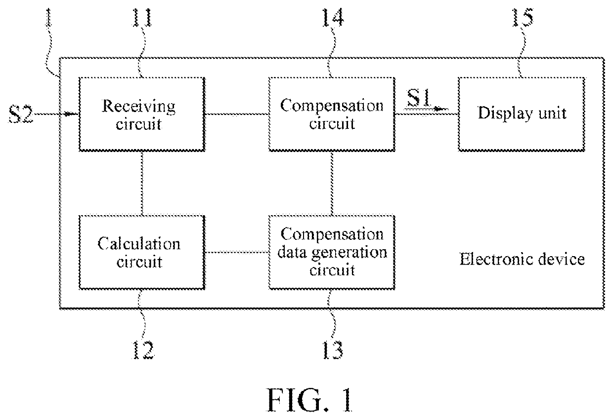
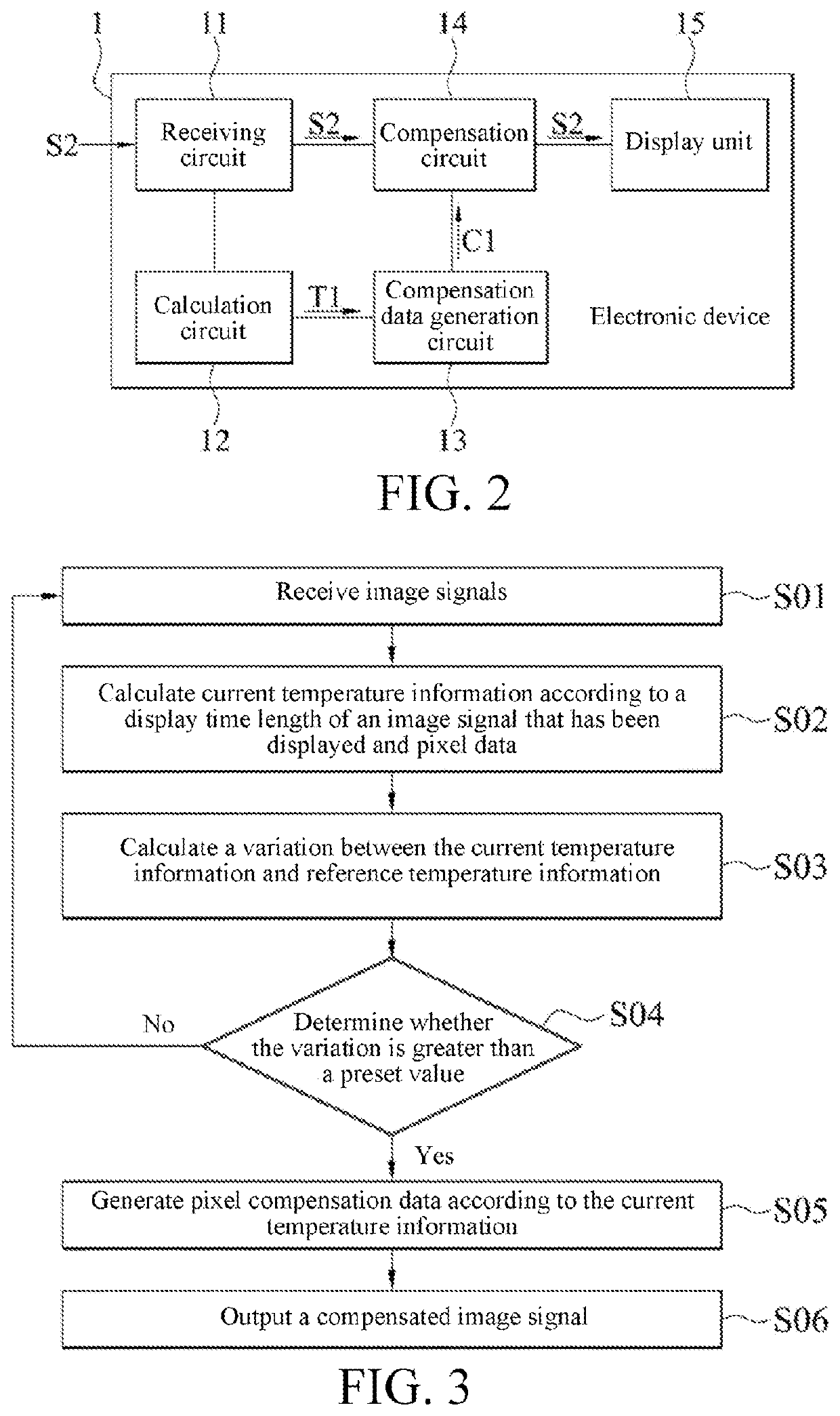
[0019]FIG. 1 is a schematic block diagram of an embodiment of an electronic device 1 according to this application. Referring to FIG. 1, the electronic device 1 includes a receiving circuit 11, a calculation circuit 12, a compensation data generation circuit 13, a compensation circuit 14, and a display unit 15. The receiving circuit 11 is coupled to the calculation circuit 12 and the compensation circuit 14. The compensation circuit 14 is coupled to the compensation data generation circuit 13 and the display unit 15. The electronic device 1 sequentially receives, at different time points, an image signal S1 and an image signal S2 generated by an image signal source. The electronic device 1 receives the image signal S1 (hereinafter referred to as a first image signal S1) first. The displ...
PUM
 Abstract
Description
Claims
Application Information


