
Display device

a display device and display technology, applied in the direction of semiconductor devices, basic electric elements, electrical equipment, etc., can solve the problems of low gray scale mura, and inability to achieve peak luminance in the blue sub-pixel

Pending Publication Date: 2022-06-30
LG DISPLAY CO LTD
View PDF0 Cites 0 Cited by
  • Summary
  • Abstract
  • Description
  • Claims
  • Application Information

AI Technical Summary

Benefits of technology

The present patent aims to improve the quality of gaming and video displays by reducing mura (an issue of uneven display) at low gray scales. The technical effect of this patent is achieved by applying a high S-factor to certain parts of the display and a low S- factor to other parts, which helps to minimize the impact of mura. Additionally, the patent allows for easy adjustment of gray scales for different sub-pixels, ensuring optimal performance.

Problems solved by technology

For example, when a high S-factor is applied to all of the sub-pixels, ranges of data voltages of the red sub-pixel and the green sub-pixel for expressing gray scale may satisfy a voltage specification of a data driver, but the blue sub-pixel may be out of the voltage specification of the data driver because the range of data voltages of the blue sub-pixel is excessively wide (e.g., thus, some gray scale values may not be supported or properly expressed by the blue sub-pixel).
In this situation, peak luminance in the blue sub-pixel may not be achieved.
In addition, when a low S-factor is applied to the plurality of sub-pixels, the blue sub-pixel may have an appropriate range of data voltages that satisfies the voltage specification of the data driver, but the ranges of data voltages of the red sub-pixel and the green sub-pixel are excessively narrower, causing mura at low gray scale (e.g., unevenness, irregularities or blemishes).

Method used


Image

  • Display device
  • Display device
  • Display device

Examples


Embodiment Construction

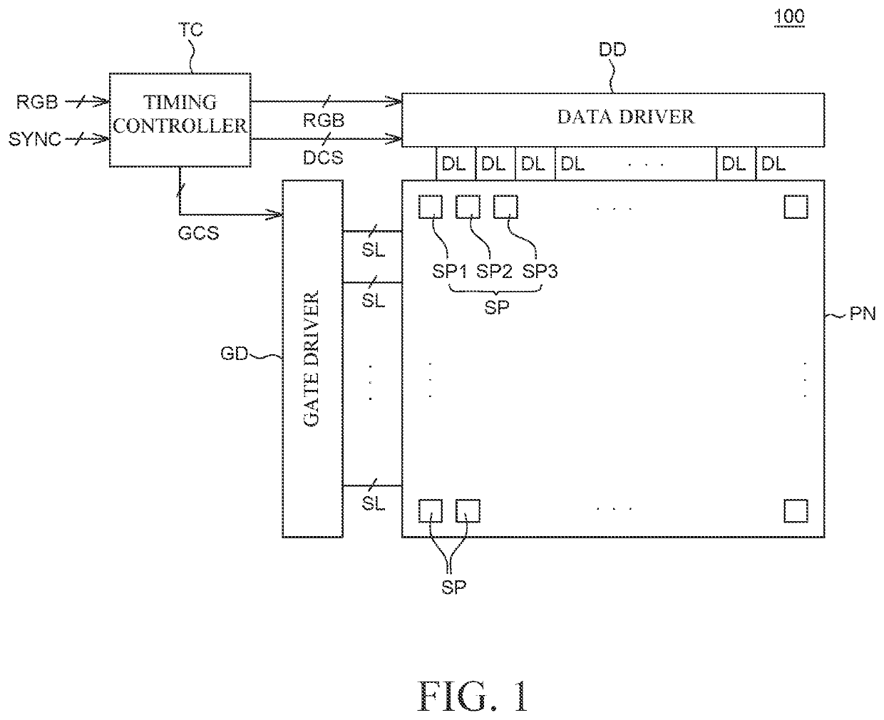
[0026]Advantages and characteristics of the present disclosure and a method of achieving the advantages and characteristics will be clear by referring to example embodiments described below in detail together with the accompanying drawings. However, the present disclosure is not limited to the example embodiments disclosed herein but will be implemented in various forms. The example embodiments are provided by way of example only so that those skilled in the art can fully understand the disclosures of the present disclosure and the scope of the present disclosure. Therefore, the present disclosure will be defined only by the scope of the appended claims.

[0027]The shapes, sizes, ratios, angles, numbers, and the like illustrated in the accompanying drawings for describing the example embodiments of the present disclosure are merely examples, and the present disclosure is not limited thereto. Like reference numerals generally denote like elements throughout the specification. Further, ...


PUM

PropertyMeasurementUnit
coloraaaaaaaaaa
areaaaaaaaaaaa
semiconductoraaaaaaaaaa

Abstract

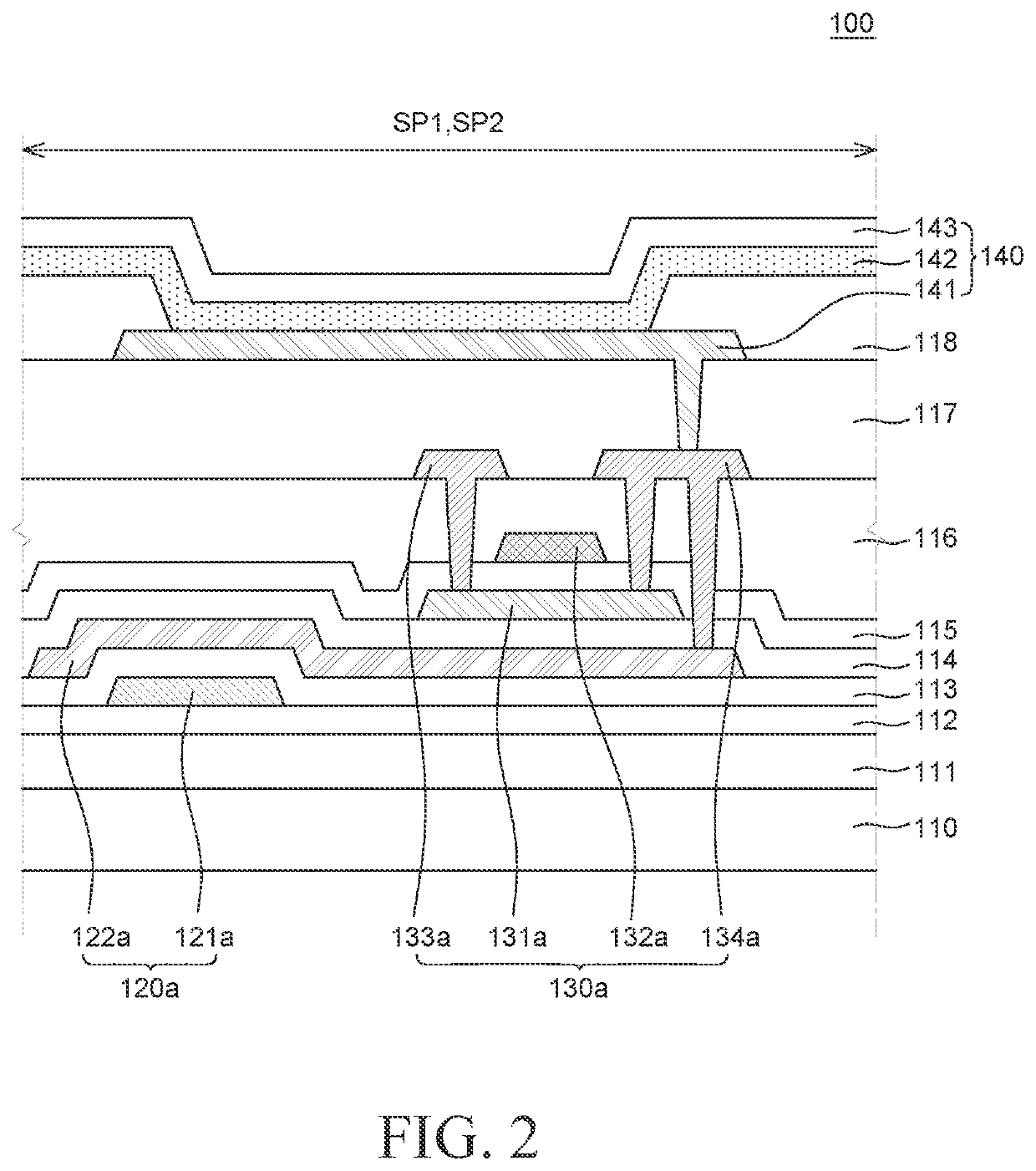
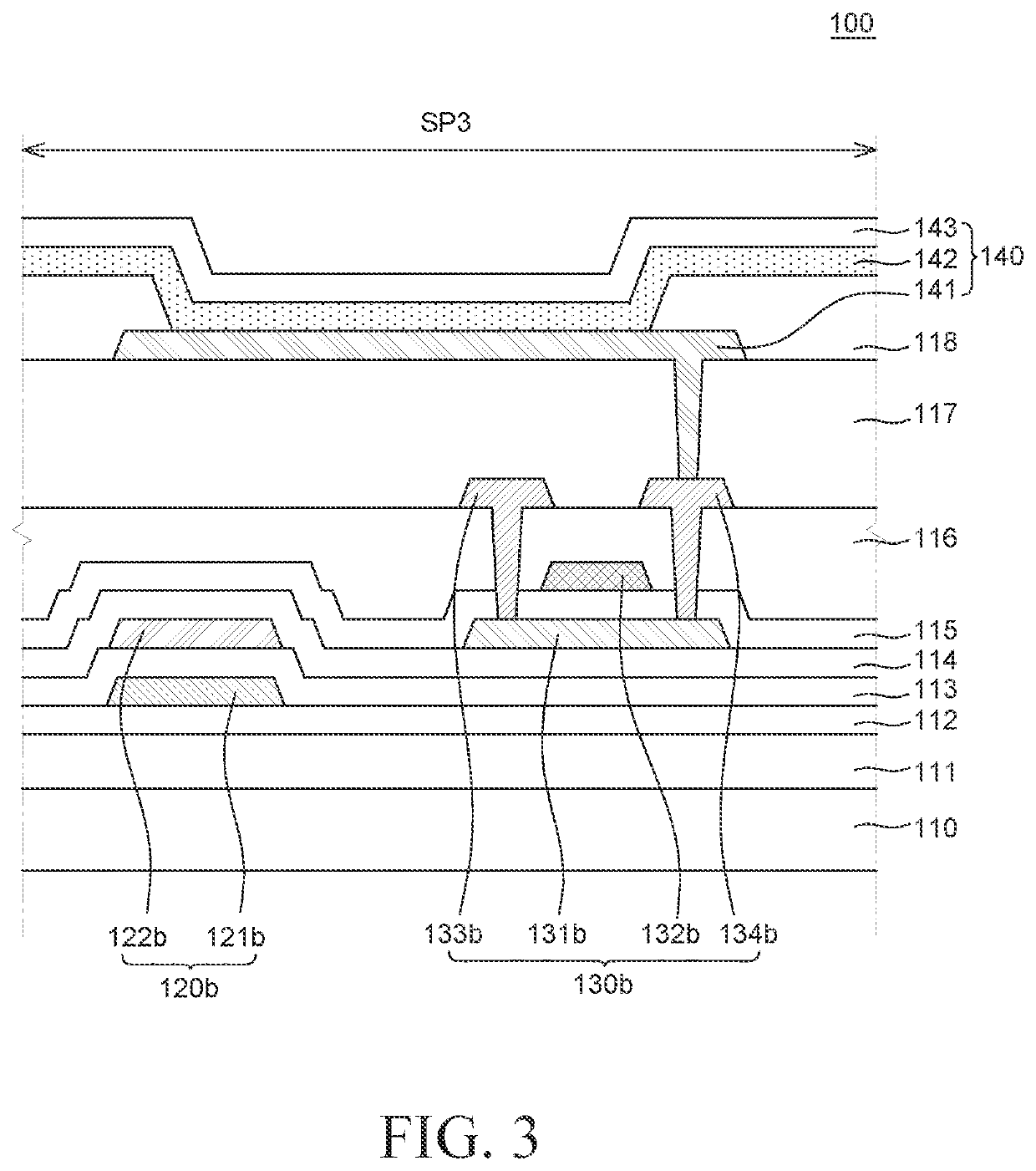
A display device can include a plurality of sub-pixels disposed on a substrate; a storage capacitor disposed in each of the plurality of sub-pixels; a buffer layer disposed on the storage capacitor; a transistor disposed on the buffer layer in each of the plurality of sub-pixels; and a light emitting element disposed on the transistor in each the plurality of sub-pixels, in which the plurality of sub-pixels include a first sub-pixel, a second sub-pixel, and a third sub-pixel, each of the first, second and third sub-pixels being configured to emit a different color of light, at least one of the plurality of sub-pixels includes a metal layer disposed below the transistor, and the metal layer is connected to one electrode of the storage capacitor.

Description

CROSS-REFERENCE TO RELATED APPLICATIONS[0001]This application claims priority to Korean Patent Application No. 10-2020-0189238 filed on Dec. 31, 2020, in the Republic of Korea, the entire contents of which are hereby expressly incorporated by reference into the present application.BACKGROUNDTechnical Field[0002]The present disclosure relates to a display device, and more particularly, to a display device capable of improving quality by applying an S-factor optimized for each sub-pixel.Discussion of the Related Art[0003]Recently, as our society advances toward an information-oriented society, the field of display devices for visually expressing an electrical information signal has rapidly advanced. Various display devices having excellent performance in terms of thinness, lightness, and low power consumption, are being developed correspondingly.[0004]Specific examples of such a display device include a liquid crystal display (LCD), and electroluminescent display devices such as an or...

Claims


Application Information

Patent Timeline
Patent Type & Authority Applications(United States)
IPC IPC(8): H01L27/32
CPCH01L27/3265H01L27/1225H01L27/3262H10K59/12H10K59/1213H10K59/1216H10K59/126H10K59/131H01L27/124H01L27/1255H10K59/35H01L29/7869
Inventor PARK, JAEHOON
Owner LG DISPLAY CO LTD
Learn More