Back-illuminated sensor with boron layer deposited using plasma atomic layer deposition

Pending Publication Date: 2022-08-11
KLA TENCOR CORP
View PDF0 Cites 0 Cited by
  • Summary
  • Abstract
  • Description
  • Claims
  • Application Information

AI Technical Summary

Benefits of technology

[0019]The present invention is directed to a method for fabricating a back-illuminated image sensor that utilizes a plasma atomic layer deposition (plasma ALD) boron layer formation process to generate a thin, pinhole-free pure boron layer over active areas of the image sensor. The present invention is also directed to back-illuminated image sensors incorporating at least one pure boron layer formed by the plasma ALD process, and to an inspection system utilizing such back-illuminated image sensor. By

Problems solved by technology

Because inspection systems are typically in use 24 hours per day with only short stoppages, the detectors are exposed to large doses of radiation after only a few months of operation.
Although it may appear such wavelength photons cannot be absorbed by silicon dioxide, silicon dioxide as grown on a silicon surface must have some dangling bonds at the interface with the silicon because the silicon dioxide structure cannot perfectly match that of the silicon crystal.
Furthermore, because the single dioxide is amorphous, there are likely also some dangling bonds within the material.
These electric fields can cause electrons created in the semiconductor by absorption of photons to migrate to the surface of the semiconductor and recombine, thereby resulting in lost signal and reduced detector quantum efficiency.
At normal operating temperatures of the detector, which are typically in a range from around room temperature to about 50° C., these changes will not recover.
In particular, it is known that conventional silicon photodiodes used as EUV detectors degrade in efficiency with use.
The silicon dioxide layer on the surface of semiconductor detectors significantly reduces the efficiency of those detectors for low-energy (less than about 2 keV) electrons.
Growing or depositing an alternative dielectric material (instead of the oxide) on the surface of the semiconductor results in a much higher density of defect states at the semiconductor to silicon dioxide interface.
These defects reduce the quantum efficiency of the detector, especially for photons or charged particles absorbed close to the surface of the semiconductor.
An additional cause of degradation of EUV sensors is that, in a EUV system, a thin layer of carbon builds up over time on any surface exposed to EUV radiation, including the surface of the image sensors and optical elements

Method used


Image

  • Back-illuminated sensor with boron layer deposited using plasma atomic layer deposition
  • Back-illuminated sensor with boron layer deposited using plasma atomic layer deposition
  • Back-illuminated sensor with boron layer deposited using plasma atomic layer deposition

Examples


Example

DETAILED DESCRIPTION OF THE DRAWINGS

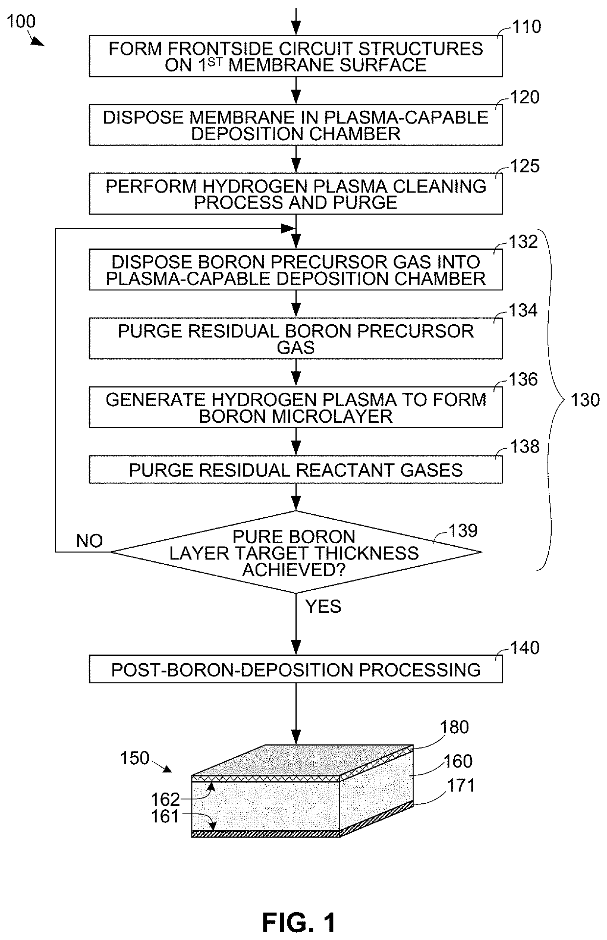
[0033]FIG. 1 is a flow diagram depicting a method 100 for producing an image sensor 150 that is configured to sense DUV / VUV / EUV radiation or charged particles using a plasma ALD boron layer formation process according to a generalized embodiment of the present invention. Image sensor 150 is partially depicted in a simplified form at the bottom of FIG. 1 for reference. Additional details related to method 100 and image sensor 150 are described below with reference to FIGS. 2A through 4B.

[0034]Referring to block 110 at the top of FIG. 1 and to image sensor 150 at the bottom of FIG. 1, front-end circuit structures 171 are generated on the frontside surface 161 of a semiconductor membrane 160 using well-known integrated circuit (IC) fabrication processes such as lithography, deposition, ion implantation, annealing and etching. As known in the art, these well-known IC fabrication processes typically include front-end processes during which non-metal st...


PUM


Abstract

Back-illuminated DUV/VUV/EUV radiation or charged particle image sensors are fabricated using a method that utilizes a plasma atomic layer deposition (plasma ALD) process to generate a thin pinhole-free pure boron layer over active sensor areas. Circuit elements are formed on a semiconductor membrane's frontside surface, and then an optional preliminary hydrogen plasma cleaning process is performed on the membrane's backside surface. The plasma ALD process includes performing multiple plasma ALD cycles, with each cycle including forming an adsorbed boron precursor layer during a first cycle phase, and then generating a hydrogen plasma to convert the precursor layer into an associated boron nanolayer during a second cycle phase. Gasses are purged from the plasma ALD process chamber after each cycle phase. The plasma ALD cycles are repeated until the resulting stack of boron nanolayers has a cumulative stack height (thickness) that is equal to a selected target thickness.

Description

RELATED APPLICATIONS / PATENTS[0001]This application claims priority from U.S. Provisional Patent Application No. 63 / 146,001, entitled “BACK-ILLUMINATED SENSOR WITH BORON LAYER DEPOSITED USING PLASMA ATOMIC LAYER DEPOSITION”, which was filed on Feb. 5, 2021.FIELD OF DISCLOSURE[0002]The present application relates to image sensors suitable for sensing radiation in deep UV (DUV), vacuum UV (VUV), and extreme UV (EUV) wavelength, and to methods for fabricating / producing such image sensors. Some embodiments of the sensors are suitable for sensing electrons and other charged particles. All of the sensors are suitable for use in photomask, reticle, or wafer inspection systems.RELATED ART[0003]The integrated circuit industry requires inspection tools with increasingly higher resolution to resolve ever smaller features of integrated circuits, photomasks, reticles, solar cells, charge coupled devices etc., as well as detect defects whose sizes are of the order of, or smaller than, those featur...

Claims


Application Information

Patent Timeline
IPC IPC(8): H01L27/146G03F7/20
CPCH01L27/14698G03F7/70033H01L27/1464G01N21/956G01N21/9501
Inventor YALAMANCHILI, SISIRFIELDEN, JOHNKOLE, FRANCISCOCHUANG, YUNG-HO ALEX
Owner KLA TENCOR CORP
Why Eureka
Try Eureka