Image display apparatus

Inactive Publication Date: 2009-04-23
HITACHI LTD
View PDF6 Cites 0 Cited by
  • Summary
  • Abstract
  • Description
  • Claims
  • Application Information

AI Technical Summary

Benefits of technology

[0014]An object of the present invention is to suppress the long-term degradation over operation time or change with the passage of time of the

Problems solved by technology

However, when the matrix electron emitter display is operated for a long time in a state in which a high voltage is applied to the acceleration electrode, a problem has arisen that a long-term degradation of the electron emission element over operation time is more serious.
Here, the long-term degradation over operation time

Method used


Image

  • Image display apparatus
  • Image display apparatus
  • Image display apparatus

Examples


Example

First Embodiment

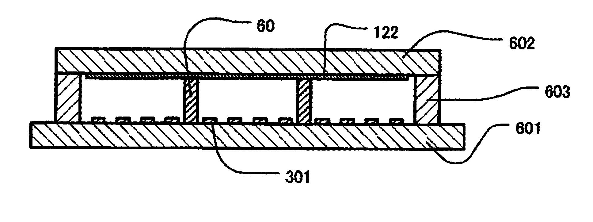
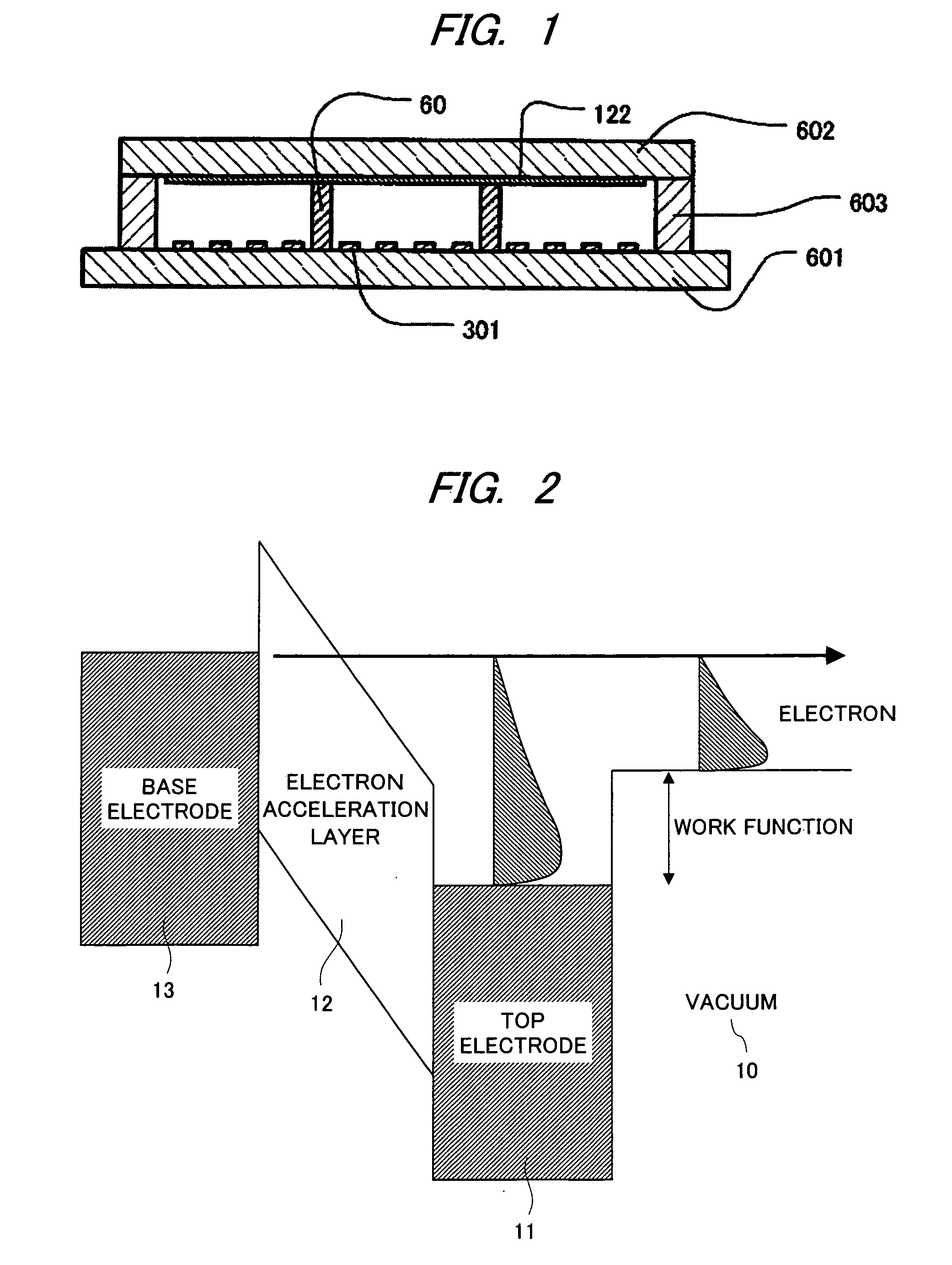
[0077]A first embodiment of the present invention is an example in a case when the present invention is applied to a MIM cathode, a surface conduction electron emitter element and the like. Here, first, a cause of degradation phenomenon of the electron emission element generated when operated in a state in which a high voltage is applied to a phosphor screen will be described.

[0078]As described in FIG. 1, the electron emitted from an electron emission element 301 is accelerated by a phosphor-screen voltage Va, and after that, is bombarded onto or irradiated at an acceleration electrode 122 and a phosphor. Here, the phosphor-screen voltage means a voltage applied to the acceleration electrode 122, and it is typically Va=3 to 12 KV. When the electron accelerated to 1 KV or more bombards the phosphor and gas molecules, it is often that the electron ionizes atoms or molecules, thereby to generate positive ion. The positive ion is accelerated by the electric field between...

Example

Second Embodiment

[0098]A second embodiment of the present invention uses a thin film electron emitter as an electron emission element. As compared with another cathode such as a field emission type cathode, the thin film electron emitter is small in spatial divergence of emitted electron beam. The reason is as follows. In the thin film electron emitter, the electron accelerated in an electron acceleration layer is emitted into vacuum from a top electrode. In the thin film electron emitter, since the top electrode and a base electrode are mutually disposed in opposition in parallel, the electric field inside the electron acceleration layer is a uniform electric field. Since the electron is accelerated by this uniform electric field, the spatial divergence of the emitted electron becomes small. That the spatial divergence of the emitted electron beam is small is favorable characteristics because a high-resolution image display apparatus can be realized.
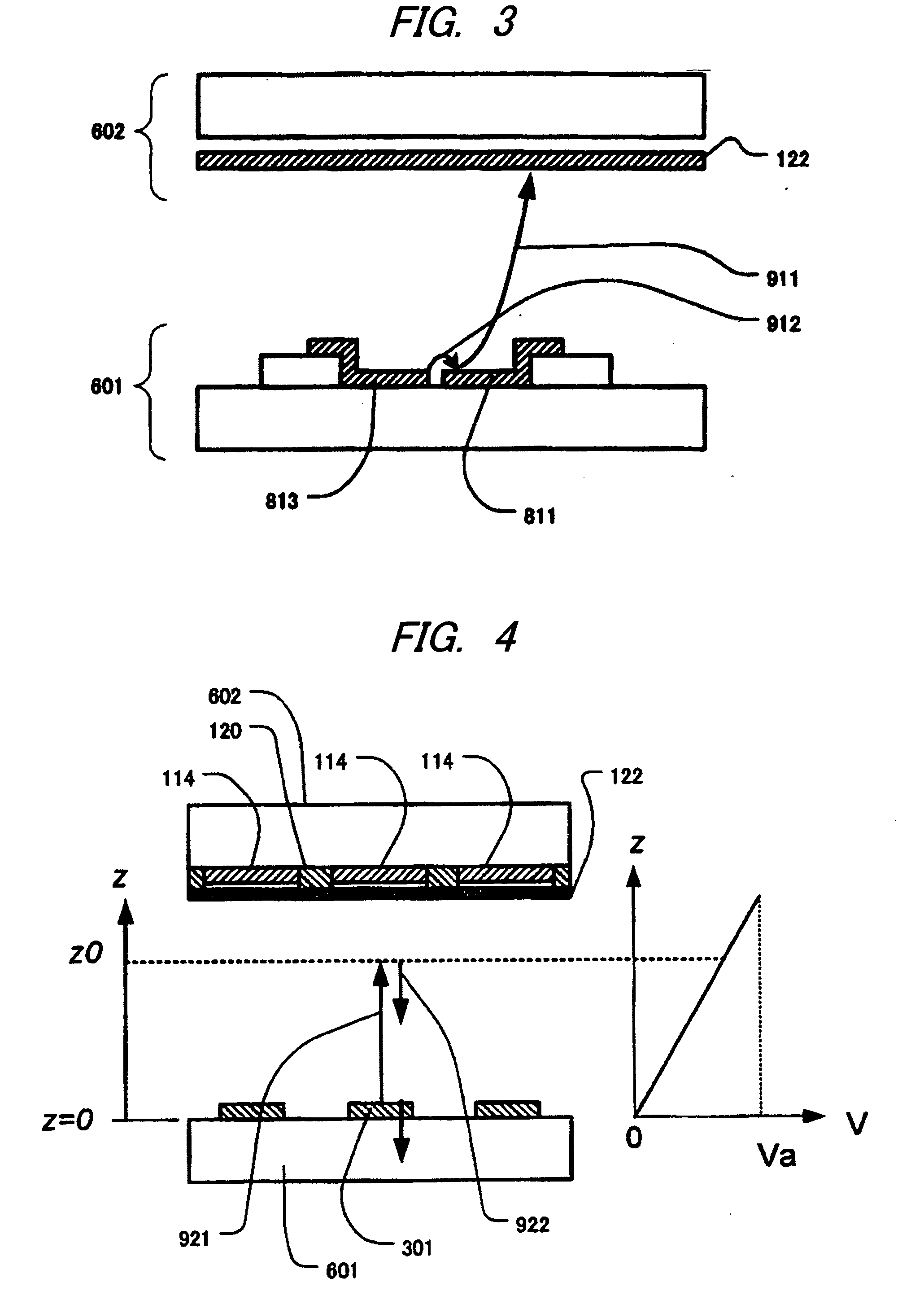
[0099]On the other hand, as evid...

Example

[0148]A third embodiment of the present invention will be described with reference to FIGS. 27 and 28A-28B. FIG. 27 is a top plan view of a cathode plate 601 constituting a display panel 100 used in the present embodiment. FIGS. 28A and 28B are cross section of the cathode plate 601, FIG. 28A is a cross section along line A-B of FIG. 27, and FIG. 28B shows a cross section along line C-D. When comparing the third embodiment with the second embodiment (FIGS. 13 and 14A-14B), the shape of a contact electrode 55 is different in the present embodiment. While the contact electrode 55 has a branch-shaped protrusion extending along the longer side of the electron emission region 35 in FIG. 13, the protrusion is not available in the present embodiment (FIG. 27).

[0149]As evident from FIG. 28B, a top electrode 11 is formed almost entirely on the surface except for a scan electrode 310 (that is, a busline electrode 32) and a deflection electrode 315. Since the film thickness (0.1 μm in the pres...


PUM


Abstract

Degradation of an electron emission element by irradiation of the positive ion generated inside a panel is suppressed. A deflection electrode is periodically disposed, and the electron emission region of an electron emission element is disposed so as not to include a center line between adjacent deflection electrodes, so that an electron beam trajectory is deflected and bombardment or irradiation of the generated positive ion to the electron emission region is prevented.

Description

CROSS-REFERENCE TO RELATED APPLICATION[0001]The present application claims priority from Japanese Patent Application No. JP 2007-270027 filed on Oct. 17, 2007, the content of which is hereby incorporated by reference into this application.TECHNICAL FIELD OF THE INVENTION[0002]The present invention relates to an image display apparatus for displaying an image by using an electron emission element and a phosphor disposed in a matrix-form.BACKGROUND OF THE INVENTION[0003]An image display device referred to also as a matrix electron emitter display takes an intersection of electrode groups orthogonal to each other as a pixel, and provides an electron emission element on each pixel, and by adjusting an applied voltage (amplitude of applied voltage) or a pulse width of an applied voltage pulse to each electron emission element, amount of emitted electrons is adjusted, and the emitted electrons are accelerated in vacuum, and after that, and bombarded onto or irradiated at the phosphor, the...

Claims


Application Information

Patent Timeline
IPC IPC(8): H01J1/62
CPCH01J29/04H01J2329/0486H01J31/127
Inventor SUZUKI, MUTSUMIKUSUNOKI, TOSHIAKI
Owner HITACHI LTD
Why Eureka
Try Eureka