Chip package and method for forming the same

Pending Publication Date: 2022-09-08
XINTEC INC
View PDF0 Cites 0 Cited by
  • Summary
  • Abstract
  • Description
  • Claims
  • Application Information

AI Technical Summary

Benefits of technology

The patent text describes a method for making a chip package by providing a substrate with a dielectric layer and a masking layer covering the dielectric layer. The masking layer has openings exposing the dielectric layer. The method includes etching the dielectric layer to form openings, and then performing a sawing process through the openings to form a chip package. The chip package includes a substrate with adjacent chip regions and a scribe-line region surrounding the chip regions. The method also includes aligning an optical element with the chip regions and the scribe-line region. The chip package has a tilted sidewall surface. The technical effects of the patent text include improved alignment accuracy and reduced damage to the substrate during the etching process.

Problems solved by technology

However, the dielectric material layer on the wafer (e.g., low-k dielectric material) is usually brittle, lacks mechanical strength, and is sensitive to thermal stress.
As a result, debris, cracks, rough sidewalls, or other types of defects within the low-k dielectric material are likely to occur during the singulation process, reducing the yield of the chip package.

Method used


Image

  • Chip package and method for forming the same
  • Chip package and method for forming the same
  • Chip package and method for forming the same

Examples


Embodiment Construction

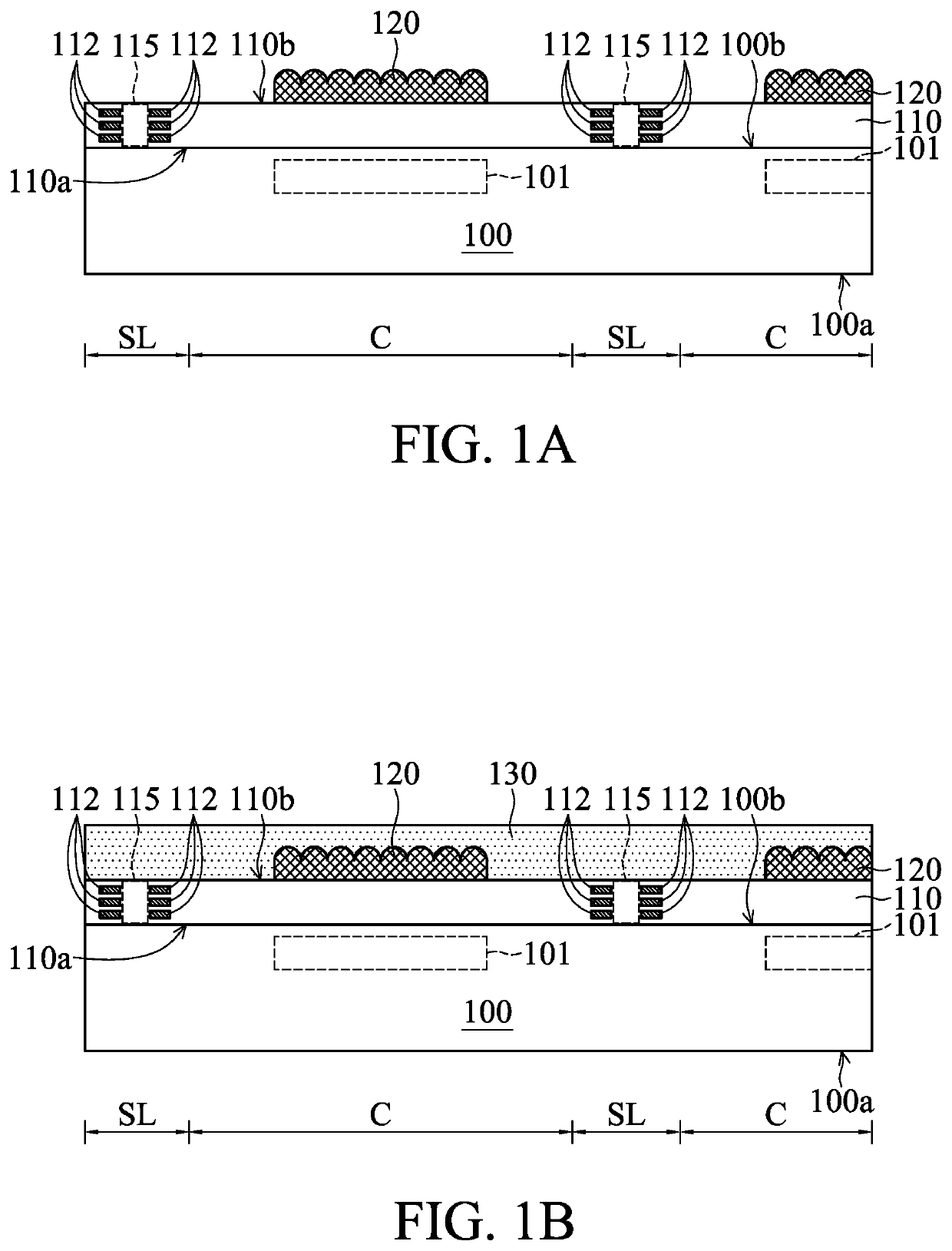
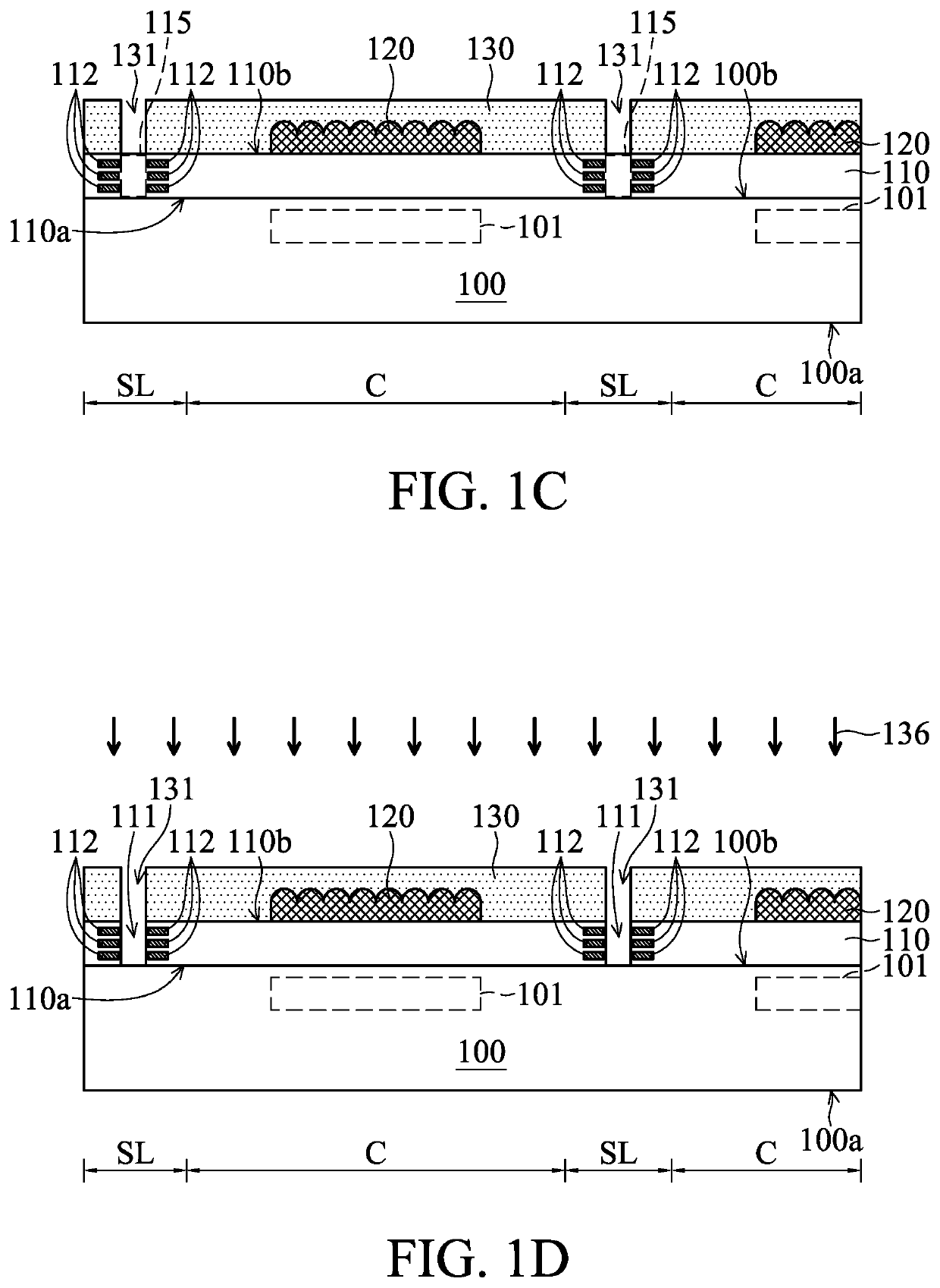
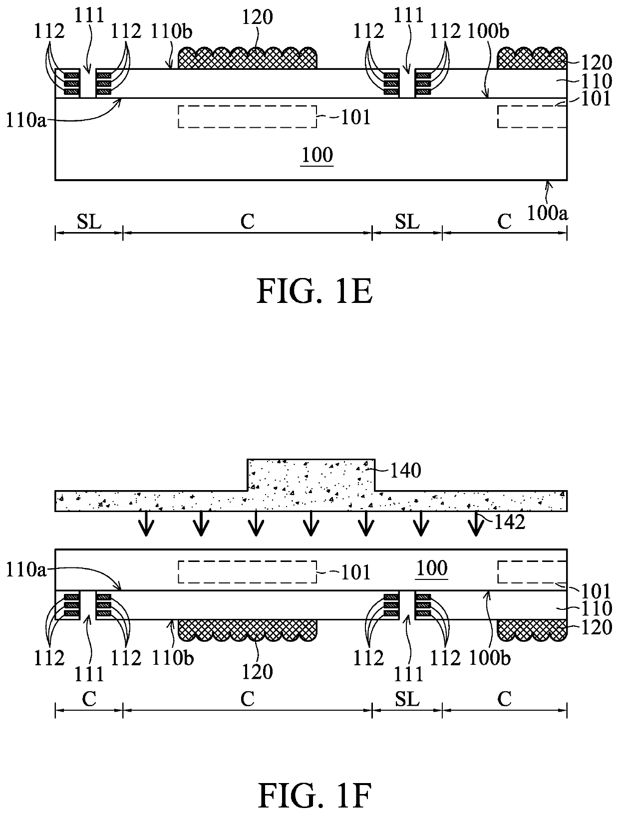
[0022]The making and using of the embodiments of the present disclosure are discussed in detail below. However, it should be noted that the embodiments provide many applicable inventive concepts that can be embodied in a variety of specific methods. The specific embodiments discussed are merely illustrative of specific methods to make and use the embodiments, and do not limit the scope of the disclosure. In addition, the present disclosure may repeat reference numbers and / or letters in the various embodiments. This repetition is for the purpose of simplicity and clarity, and does not imply any relationship between the different embodiments and / or configurations discussed. Moreover, when a first material layer is referred to as being on or overlying a second material layer, the first material layer may be in direct contact with the second material layer, or separated from the second material layer by one or more material layers.

[0023]A chip package according to some embodiments of th...


PUM


Abstract

Chip packages and methods for forming the same are provided. The method includes providing a substrate having upper and lower surfaces, and having a chip region and a scribe-line region surrounding the chip region. The substrate has a dielectric layer on its upper surface. A masking layer is formed over the substrate to cover the dielectric layer. The masking layer has a first opening exposing the dielectric layer and extending in the extending direction of the scribe-line region to surround the chip region. An etching process is performed on the dielectric layer directly below the first opening, to form a second opening that is in the dielectric layer directly below the first opening. The masking layer is removed to expose the dielectric layer having the second opening. A dicing process is performed on the substrate through the second opening.

Description

CROSS REFERENCE TO RELATED APPLICATIONS[0001]This application claims the benefit of U.S. Provisional Application No. 63 / 155,747, filed Mar. 3, 2021, the entirety of which is incorporated by reference herein.BACKGROUND OF THE INVENTIONField of the Invention[0002]The invention relates to package technology, and in particular to a chip package and a method for forming the same.Description of the Related Art[0003]Optoelectronic devices (e.g. image-sensing devices) play an important role in capturing images and have been widely used in electronic products such as digital cameras, digital video recorders, and mobile phones. The chip packaging process is an important step in the fabrication of an electronic product. Chip packages not only protect sensing chips from outside environmental contaminants, but they also provide electrical connection paths between the electronic elements inside and those outside of the chip packages.[0004]During the fabrication of the above-mentioned chip package...

Claims


Application Information

Patent Timeline
IPC IPC(8): H01L27/146H01L23/544
CPCH01L27/14698H01L23/544H01L27/14632H01L2223/5446H01L27/14683H01L27/14687H01L27/14618H01L27/14634
Inventor LIU, TSANG-YUCHANG, SHU-MINGLAI, CHAUNG-LIN
Owner XINTEC INC
Why Eureka
Try Eureka