
Eureka
For R&D, Eureka makes reading and utilizing patents & technical documents easy.
Eureka AIR
Designed for self-driven R&D workflows. Generate viable solutions, solve complex R&D challenges, empower your innovation with AI.

Eureka Materials
Designed for material experts only. Revolutionize your material R&D, from search, analyze, to developing new materials.

TechResearch
Generate reliable direction feasibility study reports for your R&D in just a few steps.

TechSeek
Discover and master advanced knowledge NOW. Basics, ideas, possibilities, all at once.

TechMind
As an expert in R&D Theories, TechMind can generates customized viable solutions instantly.

TechRisk
Analyze your overall solution with one click, know your potential R&D risks in advance.

TechMonitor
Get weekly tech updates, stay abreast of the latest tech innovations and key insights.
Optical modulator and optical transmission device using same
- Summary
- Abstract
- Description
- Claims
- Application Information
AI Technical Summary
Benefits of technology
Problems solved by technology
Method used
Image

Examples
first embodiment
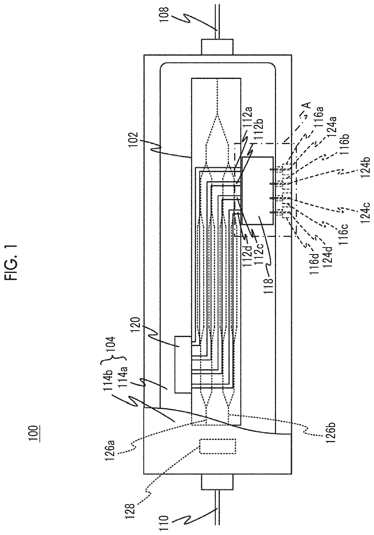
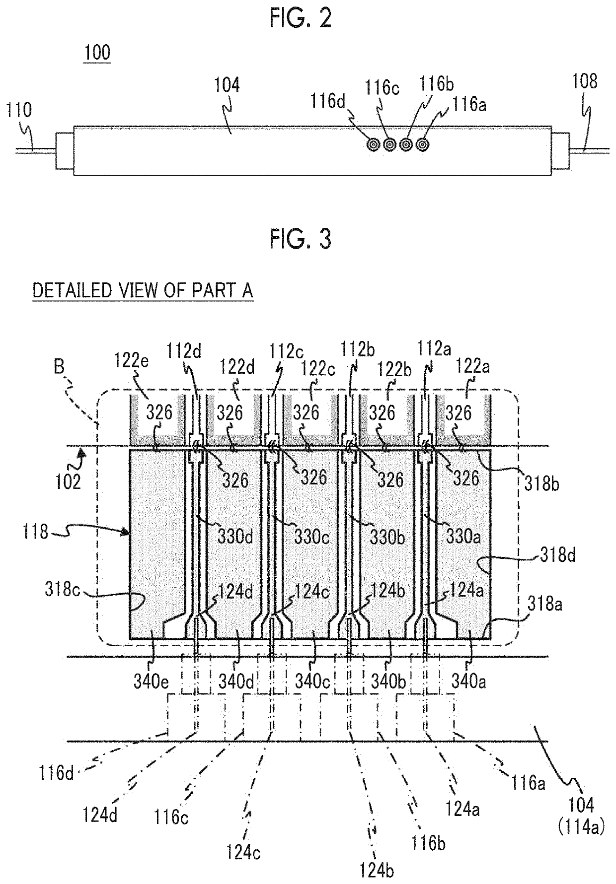
[0053]First, a first embodiment of the present invention will be described. FIG. 1 is a plan view illustrating a configuration of an optical modulator 100 according to the first embodiment of the present invention, FIG. 2 is a side view of the optical modulator 100, and FIG. 3 is a partial detail view of a part A in FIG. 1.
[0054]The optical modulator 100 includes an optical modulation element 102, a housing 104 that accommodates the optical modulation element 102, an input optical fiber 108 for inputting light into the optical modulation element 102, and an output optical fiber 110 that guides the light output from the optical modulation element 102 to an outside of the housing 104.
[0055]The optical modulation element 102 is, for example, a DP-QPSK modulator that performs optical modulation of 400 Gb / s, and includes, for example, four Mach-Zehnder type optical waveguides provided on an LN substrate. The four Mach-Zehnder type optical waveguides are provided with four signal electrod...
first modification example
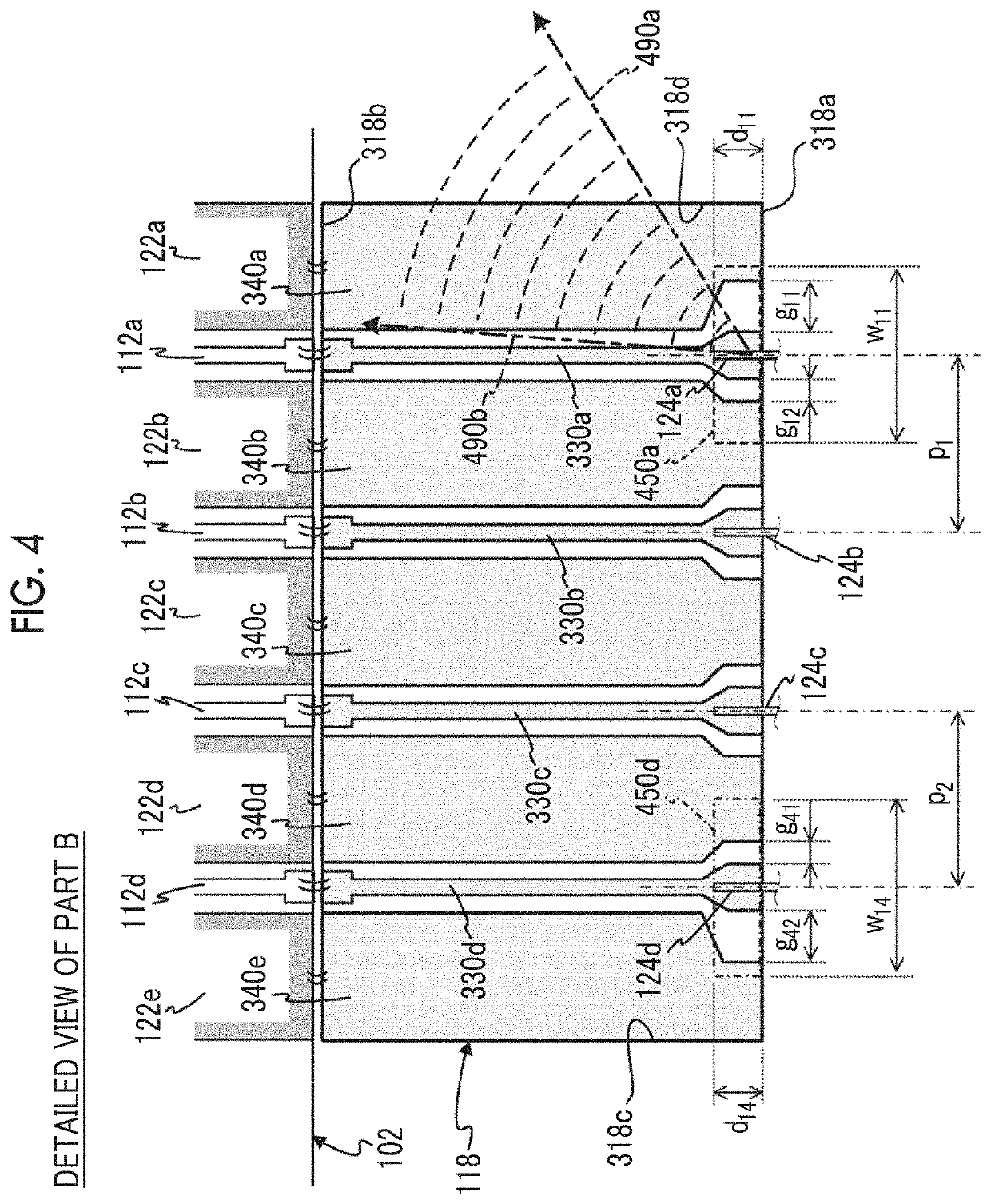
[0087]FIG. 5 is a diagram illustrating a configuration of a relay substrate 518 according to a first modification example, and is a diagram corresponding to the partial detail view of the first embodiment illustrated in FIG. 4. The relay substrate 518 can be used instead of the relay substrate 118 in the optical modulator 100 illustrated in FIG. 1. In FIG. 5, the same reference numerals as those in FIG. 4 are used for the same components as those of the components of the relay substrate 118 illustrated in FIG. 4, and the above description of FIG. 4 is adopted.
[0088]The relay substrate 518 has the same configuration as the relay substrate 118, but has a difference that a ground conductor pattern 540c is provided instead of the ground conductor pattern 340c. Thus, in the relay substrate 518, in addition to the signal conductor patterns 330a and 330d, regarding the signal conductor patterns 330b and 330c, in connection areas 550b and 550c defined for these signal conductor patterns 330...
second modification example
[0101]FIG. 6 is a diagram illustrating a configuration of a relay substrate 618 according to a second modification example, and is a diagram corresponding to the partial detail view of the first embodiment illustrated in FIG. 4. The relay substrate 618 can be used instead of the relay substrate 118 in the optical modulator 100 illustrated in FIG. 1. In FIG. 6, the same reference numerals as those in FIGS. 4 and 5 are used for the same components as those of the components of the relay substrates 118 and 518 illustrated in FIGS. 4 and 5, and the above descriptions of FIGS. 4 and 5 are adopted.
[0102]The relay substrate 618 is formed with the signal conductor patterns 330, in the same manner as the relay substrates 118 and 518. Therefore, in the relay substrate 618, the connection areas 450a, 550b, 550c, and 450d are defined for each of the signal conductor patterns 330, in the same manner as the relay substrate 518.
[0103]The relay substrate 618 has the same configuration as the relay ...
PUM
 Abstract
Description
Claims
Application Information
 - R&D Engineer
- R&D Manager
- IP Professional
- Industry Leading Data Capabilities
- Powerful AI technology
- Patent DNA Extraction
Browse by: Latest US Patents, China's latest patents, Technical Efficacy Thesaurus, Application Domain, Technology Topic, Popular Technical Reports.
© 2024 PatSnap. All rights reserved.Legal|Privacy policy|Modern Slavery Act Transparency Statement|Sitemap|About US| Contact US: help@patsnap.com