Method for obtaining a high dynamic range read-out signal of a CMOS-based pixel structure and such CMOS-based pixel structure

a pixel structure and high dynamic range technology, applied in the field of high dynamic range readout signal such cmos-based pixel structure, can solve the problem of limited dynamic range of cmos-based pixel structur

Inactive Publication Date: 2000-01-04
SEMICON COMPONENTS IND LLC
View PDF22 Cites 102 Cited by
  • Summary
  • Abstract
  • Description
  • Claims
  • Application Information

AI Technical Summary

Benefits of technology

The method is more particularly performed by the following sequence:

Problems solved by technology

This means that their dynamic range is limited by the dynamic range of the linear response.

Method used


Image

  • Method for obtaining a high dynamic range read-out signal of a CMOS-based pixel structure and such CMOS-based pixel structure
  • Method for obtaining a high dynamic range read-out signal of a CMOS-based pixel structure and such CMOS-based pixel structure
  • Method for obtaining a high dynamic range read-out signal of a CMOS-based pixel structure and such CMOS-based pixel structure

Examples


Embodiment Construction

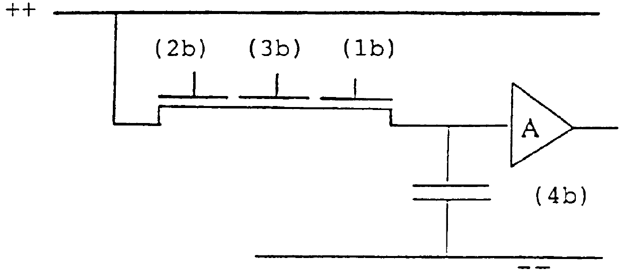
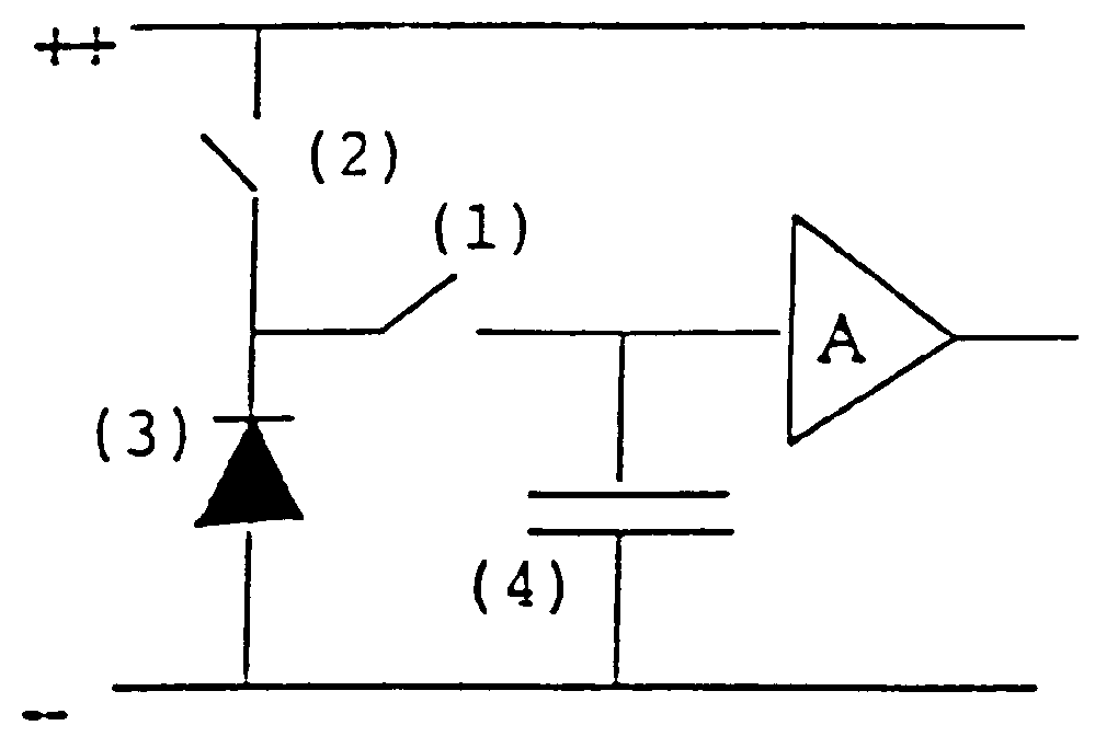
FIG. 1a represents a functional pixel structure according to an embodiment of the invention wherein a memory element (4) is provided. In this FIG. 1, (3) is a photosensitive element such as a photoreceptor or photodiode, which can be reset by a switch (2). The signal generated by the photodiode can be periodically sampled by another switch (1) on a capacitor (4). The resulting voltage can then be multiplexed in a classical way over circuitry represented by the amplifier A. FIG. 1b depicts alternative embodiments with reference numerals (with a "b" subreference) tracking reference numerals of FIG. 1a referencing corresponding elements. The discussion of FIG. 1a applies to FIG. 1b.

According to one preferred embodiment, such amplifier A is placed within the pixel structure in order to have an active pixel. According to another preferred embodiment, the amplifier A can be placed outside of the pixel structure in order to have a passive pixel structure.

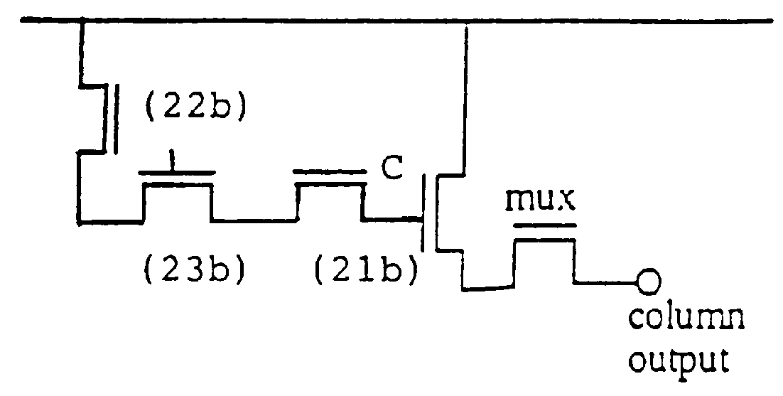
This pixel structure is able to per...


PUM


Abstract

A method is disclosed for obtaining a read-out signal of a MOS-based pixel structure having at least a photosensitive element with an output node and a memory element with a first switch therebetween. The method comprises the steps of while acquiring charge carriers on said output node of said photosensitive element, said charge carriers being converted from electromagnetic radiation on the photosensitive element, after a first time period creating a first signal, and after a second time period, creating a second signal, said read-out signal being a combination of at least said first and said second signals. According to the present invention, there is no limitation to the amount of collected charges in none of the integrated periods. The signal collected during the first period is memorized by a switch which shortly opens and closes between the period. The switch is thus in the same state in both period of time. After a second period, there are thus two charge packets, each obtained during a different time. In order to read-out, these two charge packets are then combined into one reading. This combination is known either by adding or subtracting this charge packets, e.g., by adding or subtracting them in the circuitry external to the sensor.

Description

The present invention relates to solid state imaging devices being manufactured in a CMOS- or MOS-technology. More particularly, the present invention is related to a method of obtaining a read-out signal of a CMOS-based pixel structure with a large dynamic range. The present invention is also related to a new pixel structure and to imaging devices having such pixel structure involved in the method of the present invention.BACKGROUND OF THE INVENTION AND PROBLEM DEFINITIONSolid state imaging devices are well known. These devices find a widespread use in camera systems. In such application, a matrix of pixels comprising light sensitive elements constitutes an image sensor, which is mounted in the camera system. The signal of said matrix is measured and multiplexed to a video-signal.Commonly solid state image devices are implemented in a CCD-technology or in a CMOS- or MOS-technology.Among the image sensors implemented in a CMOS- or MOS-technology, CMOS or MOS image sensors with passi...

Claims


Application Information

Patent Timeline
Patent Type & Authority Patents(United States)
IPC IPC(8): H01L27/146H04N3/15H04N5/355H04N5/374
CPCH01L27/14643H04N3/155H04N25/575
Inventor DIERICKX, BARTSCHEFFER, DANNY
Owner SEMICON COMPONENTS IND LLC
Why Eureka
Try Eureka