Stress reduction for flip chip package

a flip chip and stress reduction technology, applied in the field of integrated circuits, can solve the problems of exaggerated device footprint, low stress, and low strength of the solvent bond, and achieve the effect of reducing the stress of the soldering

Inactive Publication Date: 2000-01-04
STMICROELECTRONICS SRL
View PDF4 Cites 43 Cited by
  • Summary
  • Abstract
  • Description
  • Claims
  • Application Information

AI Technical Summary

Problems solved by technology

High temperature applications, however, often cover the top of the flip chip with a heat sink.
It also provides a modicum of mechanical strength, but the solder bonds are typically not very strong.
The problem is fur

Method used


Image

  • Stress reduction for flip chip package
  • Stress reduction for flip chip package
  • Stress reduction for flip chip package

Examples


Embodiment Construction

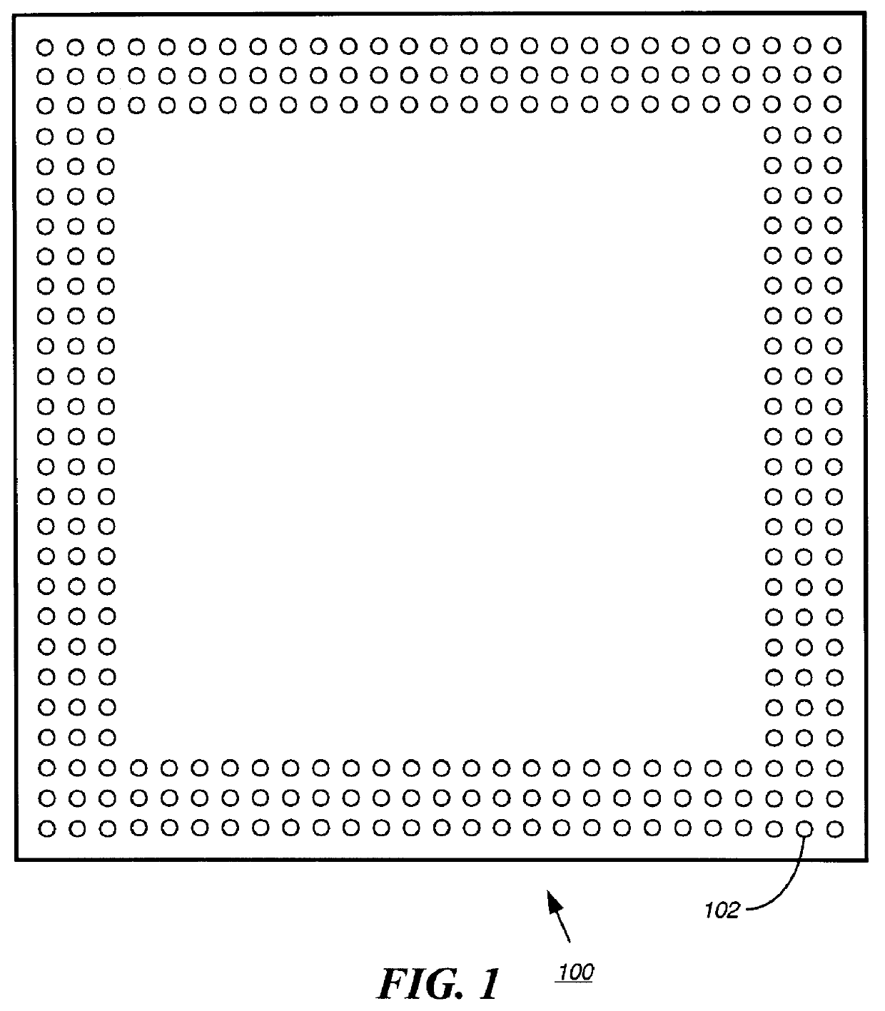
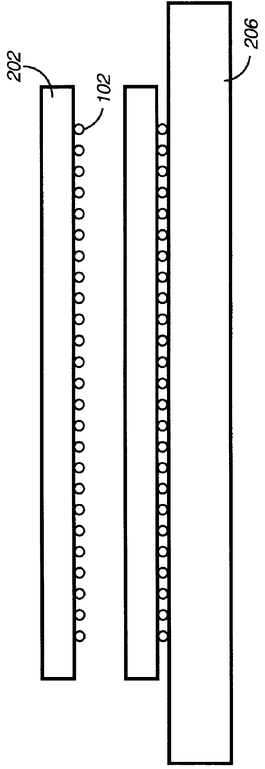
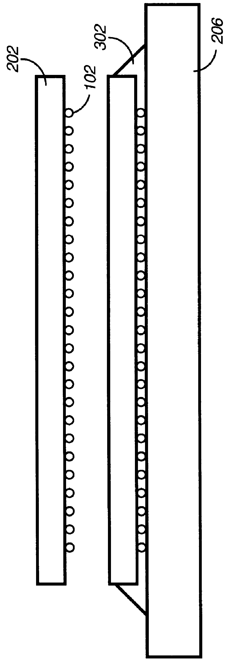
The problems associated with current flip chip assemblies can be remedied, at least partially, by anchoring the IC to the underfill layer. FIG. 7 shows the IC surface 100 with a hole 702 in each corner. FIG. 8 shows a cross-sectional view of the holes 702 and highlights a circular area 802 that is exploded in FIG. 9. FIG. 9 shows the underfill layer 302 filling the hole 702, and thereby providing an anchor.

The hole 702 can be more generally referred to as an anchoring point. An anchoring point can have virtually any shape and size. The preferred embodiment, shown in FIGS. 7-9, employs a cylindrical region with a top view of a circle, in which the anchoring point operates like a rivet. The placement of the anchoring points in the corners is effective in providing strength because the stress is greatest at the corners, as explained earlier. Other embodiments could employ an anchoring point with a top view of a rectangle, of an L-shaped region in a comer, or of an arc placed in a corne...


PUM


Abstract

The bond between a flip chip integrated circuit and a substrate is subject to mechanical stress from thermal cycles. This problem is exaggerated when the substrate has a rate of thermal expansion which is appreciably different from that of silicon. This problem is further exaggerated when the IC has a large footprint because it will experience a larger absolute expansion. A solution is proposed to this problem which involves creating an anchoring point. The anchoring point can be in either the IC or the substrate and can be a through-hole or a surface indentation such as a groove or a cutout. The anchoring point is filled with the underfill material during the underfill process. The anchoring point thus provides additional mechanical strength to the bond between the IC and the substrate.

Description

Not applicable.1. Field of the InventionThe invention disclosed broadly relates to the field of integrated circuits, and more particularly relates to the field of assembly technologies for IC flip chip packages. The invention provides a mechanism for reducing the incidence of delamination due to thermal cycling stress.2. Description of the Prior ArtThe standard method of connecting integrated circuits ("ICs") to a substrate uses conventional wire-bonding technology. The IC is glued, or otherwise fixed, to the substrate with the circuit facing up and away from the substrate. Perimeter gold wire is then typically used to connect the circuit to the substrate.An alternative to the standard interconnect method is flip chip technology. With a flip chip the IC is turned over ("flipped") so that the circuit faces the substrate. Circuit connections can now be accessed directly on the face and do not need to be routed to the perimeter of the IC. The classic method of interconnecting the circu...

Claims


Application Information

Patent Timeline
IPC IPC(8): H01L21/56H01L21/02H01L29/06H01L29/02H01L21/60
CPCH01L21/563H01L24/28H01L29/0657H01L2924/07811H01L2224/16145H01L2224/16225H01L2224/73203H01L2224/73204H01L2224/83102H01L2224/92125H01L2924/01004H01L2924/01005H01L2924/01033H01L2924/01079H01L2924/01082H01L2924/10157H01L2924/10158H01L2924/14H01L2924/15151H01L2924/18301H01L2924/30107H01L2924/3511H01L2924/01006H01L2924/00H01L2924/12042H01L2224/45144
Inventor CHIU, ANTHONY
Owner STMICROELECTRONICS SRL
Why Eureka
Try Eureka