Eureka AIR delivers breakthrough ideas for toughest innovation challenges, trusted by R&D personnel around the world.

Coupled microstrip lines

Inactive Publication Date: 2000-01-18
MURATA MFG CO LTD
View PDF6 Cites 5 Cited by
  • Summary
  • Abstract
  • Description
  • Claims
  • Application Information

AI Technical Summary

Problems solved by technology

However, in the aforesaid prior art, it is impossible to make the space between two microstrip lines smaller than the smallest space which is obtainable by a conventional electrode forming process, because light enters the area under the photomask which should remain unexposed, to produce the space between the two microstrip lines, when the resist adjacent to the photomask is exposed.
Accordingly, the area under the photomask is also exposed and it is impossible to produce the space.
Therefore, the degree of coupling between the microstrip lines, which depends on the space therebetween, is limited by the electrode forming process.

Method used


Image

  • Coupled microstrip lines
  • Coupled microstrip lines
  • Coupled microstrip lines

Examples


Embodiment Construction

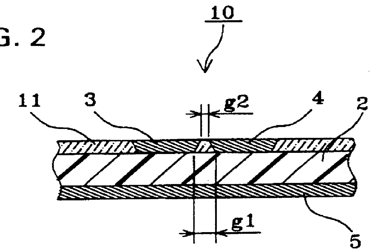
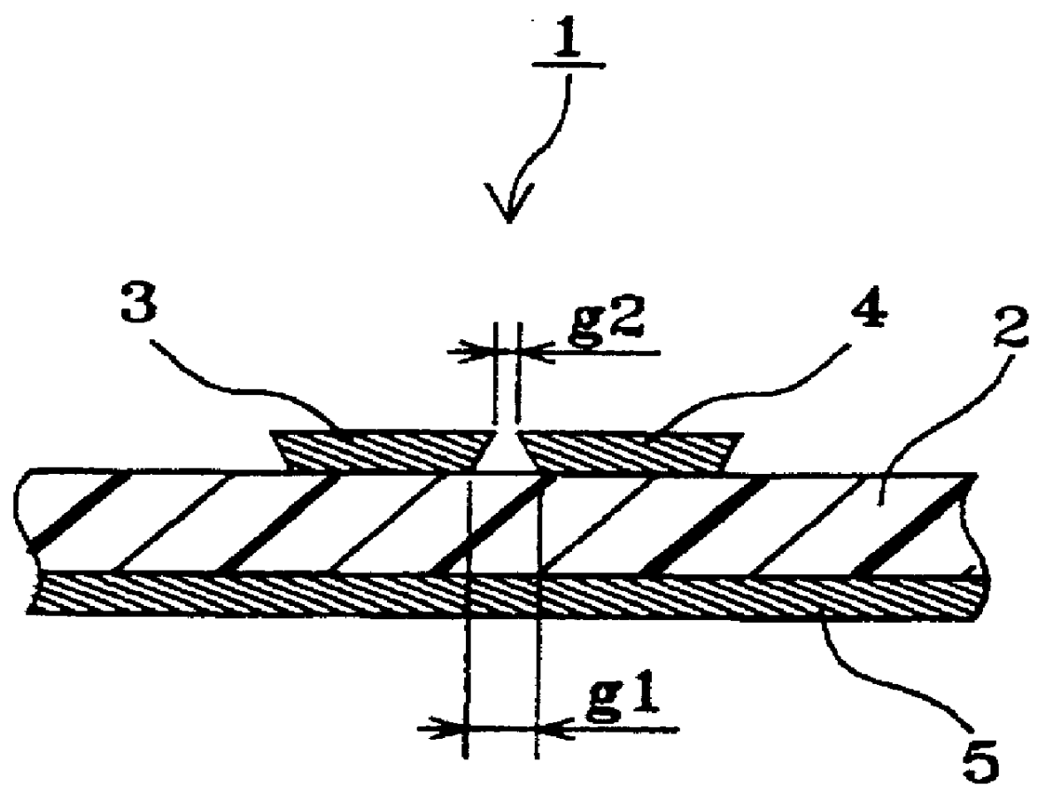
FIG. 1 is a cross-sectional view of a coupled line according to an embodiment of the present invention. Referring to FIG. 1, a coupled line 1 comprises a dielectric substrate 2, two parallel and close microstrip lines 3 and 4, and a ground electrode 5. The microstrip lines 3 and 4 are arranged with a space g1 therebetween, which is the smallest possible space that can be obtained in a conventional electrode forming process, at the bottom sides thereof in contact with the dielectric substrate 2, and are arranged for being electromagnetically coupled to each other.

The microstrip lines 3 and 4 have a cross-section shaped like a trapezoid which is wide at the top side and narrow on the bottom side which is in contact with the dielectric substrate 2. Therefore, a space g2 between the microstrip lines 3 and 4 at the top side is smaller than the smallest possible space g1 therebetween which is obtainable in the conventional electrode forming process.

Such formation of the coupled line allow...


PUM

PropertyMeasurementUnit
Dielectric polarization enthalpyaaaaaaaaaa
Electrical conductoraaaaaaaaaa

Abstract

In a coupled line, microstrip lines are formed so as to be arranged with a spacing that is narrower than the smallest possible space that is obtainable with a conventional electrode forming process, on a top side thereof spaced away from a dielectric substrate. The microstriplines have a trapezoid-shaped cross-section with the narrower major surface at the bottom, in contact with the dielectric substrate. Such formation makes it possible to strengthen the coupling between the microstrip lines, and to reduce the conductor loss of the microstrip lines.

Description

1. Field of the InventionThe present invention relates to a coupled line, and more particularly, to a coupled line for use at high frequencies.2. Description of the Related ArtFIG. 4 is a cross-sectional view of a conventional coupled line including microstrip lines. Referring to FIG. 4, a coupled line 20 comprises a dielectric substrate 21, microstrip lines 22 and 23, and a ground electrode 24. The microstrip lines 22 and 23 have a rectangular cross-section, are arranged with a space g3 therebetween, and are electromagnetically coupled to each other.However, in the aforesaid prior art, it is impossible to make the space between two microstrip lines smaller than the smallest space which is obtainable by a conventional electrode forming process, because light enters the area under the photomask which should remain unexposed, to produce the space between the two microstrip lines, when the resist adjacent to the photomask is exposed. Accordingly, the area under the photomask is also ex...

Claims


Application Information

Patent Timeline
IPC IPC(8): H01P11/00H01P5/16H01P5/18H05K1/02H05K3/04H05K3/18H05K3/02H01L23/52H01L21/3205H01L27/01H01P5/02
CPCH01P5/185H01P11/00H05K1/0239H05K1/0242H05K1/0228Y10T29/49124H05K3/184H05K2201/09236H05K2201/098H05K2201/09881H05K3/048
Inventor SASAKI, YUTAKANAKANISHI, HIDEFUMITANAKA, HIROAKI
Owner MURATA MFG CO LTD
Why Eureka
Eureka Blog
Learn More