Semiconductor integrated circuit having standard and custom circuit regions

a technology of integrated circuits and custom circuits, which is applied in the direction of semiconductor devices, semiconductor/solid-state device details, electrical devices, etc., can solve the problems of limited ability to shorten the time for manufacturing products, inability to allow further shortening of manufacturing time, and difficulty in obtaining the substantive effect of the above shortening of time-period

Inactive Publication Date: 2000-03-14
NEC ELECTRONICS CORP
View PDF12 Cites 16 Cited by
  • Summary
  • Abstract
  • Description
  • Claims
  • Application Information

AI Technical Summary

Problems solved by technology

It is limited in ability to shorten the time for manufacturing of the product.
The above conventional type of the semiconductor integrated circuit having the standard and custom circuit regions does not allow further shortening of the manufacturing time.
If the custom circuit region is large relative to the standard circuit region, then it is difficult to obtain a substantive effect of the above shortening of the time-period from receipt of the user's order to the delivery of the product.
This, however, substantially limits the responsibility and freedom to the customization.
This results in enlargement in total size of the product and also makes it difficult to increase the density of integration of the circuits.

Method used


Image

  • Semiconductor integrated circuit having standard and custom circuit regions
  • Semiconductor integrated circuit having standard and custom circuit regions
  • Semiconductor integrated circuit having standard and custom circuit regions

Examples


first embodiment

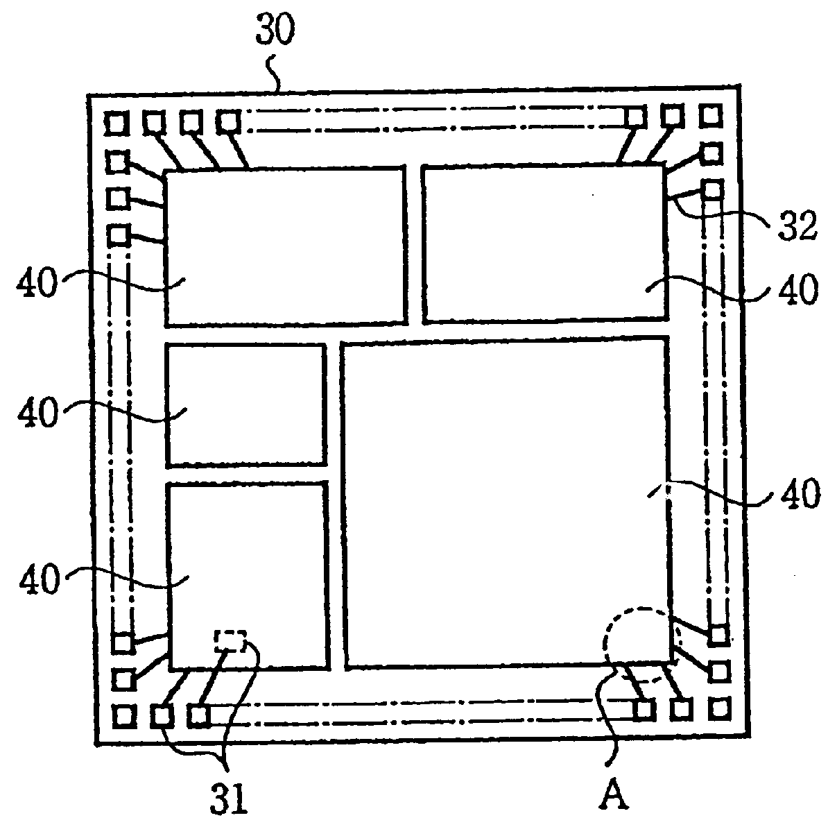
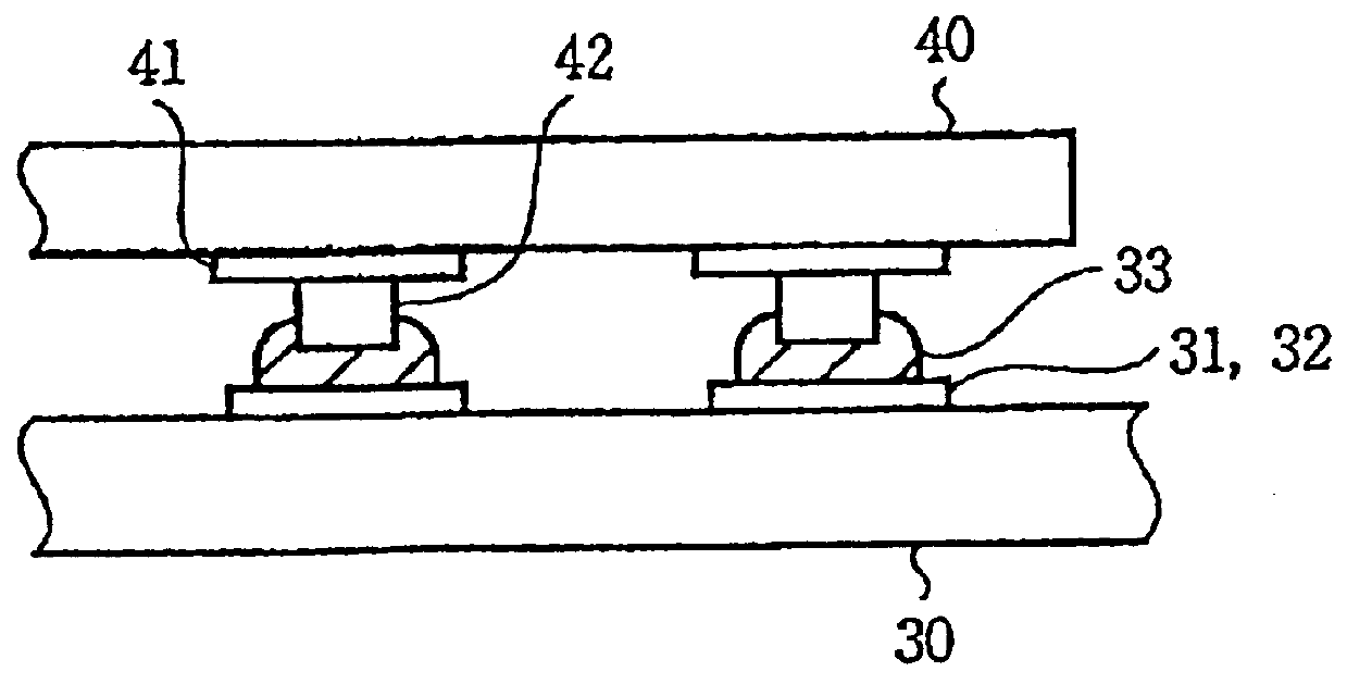
A first embodiment according to the present invention will be described with reference to FIGS. 3A and 3B. FIG. 3A is a plane view illustrative of a novel integrated circuit having standard and custom circuit regions. FIG. 3B is a partially enlarged cross sectional elevation view illustrative of connections between an option chip and a mother chip via bumps in an A-region in FIG. 3A. A mother chip 1 has a peripheral region on which a plurality of electrode pads 12 are provided along each side of the mother chip 1. A standard circuit region is provided which is surrounded by the peripheral region. A custom circuit region is partially provided in the standard circuit region. The standard circuit region has basic / common circuits 11 which are standardized for basic and common purposes and functions. The custom circuit region has an option chip connection region 15. The option chip connection region 15 has a plurality of bump electrodes 14. An option chip 2 is mounted on the option chip ...

second embodiment

A second embodiment according to the present invention will be described with reference to FIGS. 4A and 4B. FIG. 4A is a plane view illustrative of option chips mounted on a mother chip. FIG. 4B is a fragmentary cross sectional elevation view illustrative of connections between an option chip and a mother chip via bumps in FIG. 4A. The structure of the semiconductor integrated circuit chip is substantially the same as in the first embodiment except for a protection buffer layer 3 being provided between the mother chip 1 and the option chip 2. A mother chip 1 has a peripheral region on which a plurality of electrode pads are provided along each side of the mother chip 1. A standard circuit region is provided which is surrounded by the peripheral region. A custom circuit region is partially provided in the standard circuit region. The standard circuit region has basic / common circuits which are standardized for basic and common purposes and functions. The custom circuit region has an o...

third embodiment

A third embodiment according to the present invention will be described with reference to FIGS. 5A and 5B. FIG. 5A is a schematic and fragmentary cross sectional elevation view illustrative of a short calipers alignment between an option chip and a mother chip. FIG. 5B is a plane view illustrative of short calipers provided in an option chip. As the scaling down of the integrated circuit chip is required, then it is also required to narrow the pitch of the bump electrodes 14 and 21. Under this condition, a highly accurate alignment between the mother chip 1 and the option chip 2 is required. Since further the distance between the mother chip 1 and the option chip 2 is narrow, then it is difficult to confirm that the corresponding pairs of the bump electrodes 14 and 21 are correctly positioned to be bonded to each other. For those reasons, it is effective to use the principle of the calipers. For example, as illustrated in FIG. 5A, a plurality of short caliper portions 23x and 23y ar...


PUM


Abstract

A semiconductor device includes a mother chip having a standard integrated circuit and electrodes pads, and an option chip having a custom integrated circuit, the option chip being provided over a part of the mother chip via connectors.

Description

The present invention relates to a semiconductor integrated circuit, and more particularly to a semiconductor integrated circuit having both a standard circuit region and a custom circuit region which is customized for the user's requirement.DESCRIPTION OF THE RELATED ARTThe semiconductor integrated circuit integrated on a single chip often have both a standard circuit region and a custom circuit region which is customized for the user's requirement. The standard circuit region has basic and fundamental circuits which are standardized for common and basic purposes and functions. By contrast, the custom circuit region has modified and additional circuits which are customized for different and specific purposes and functions. In recent years, the majority of the semiconductor integrated circuits is the type as described above.One of the conventional semiconductor integrated circuit having both standard and custom circuit regions will be described with reference to FIG. 1 which is a pl...

Claims


Application Information

Patent Timeline
Patent Type & Authority Patents(United States)
IPC IPC(8): H01L25/065H01L27/02H01L25/18H01L21/822H01L25/07H01L27/01H01L27/04
CPCH01L25/0657H01L25/18H01L27/0207H01L2225/06513H01L2225/06555H01L2225/06593H01L2224/16H01L24/13H01L24/16H01L24/17H01L24/81H01L25/50H01L2224/10135H01L2224/10165H01L2224/1403H01L2224/14517H01L2224/81136H01L2224/81141H01L2224/83365H01L2224/83385H01L23/50
Inventor TAJIMA, KAZUHISA
Owner NEC ELECTRONICS CORP
Why Eureka
Try Eureka