
Wide exclusive or and wide-input and for PLDS

a wide-input, wide-output technology, applied in the direction of computation using denominational number representation, pulse technique, instruments, etc., can solve the problems of device limitations, high cost, slow implementation speed, etc., and achieve efficient and fast wide-output capability and more logic flexibility.

Inactive Publication Date: 2000-03-28
ALTERA CORP
View PDF11 Cites 26 Cited by
  • Summary
  • Abstract
  • Description
  • Claims
  • Application Information

AI Technical Summary

Benefits of technology

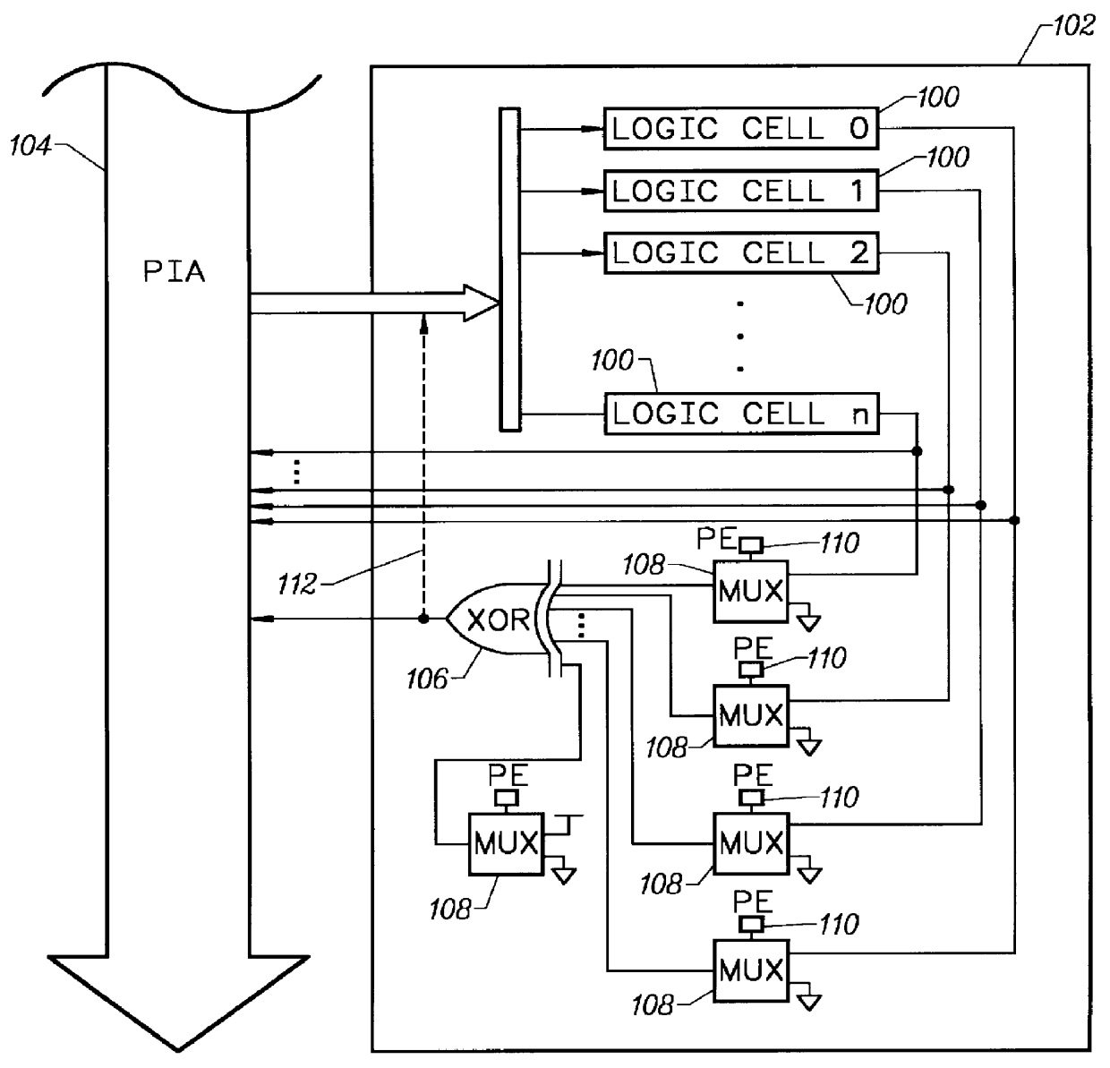
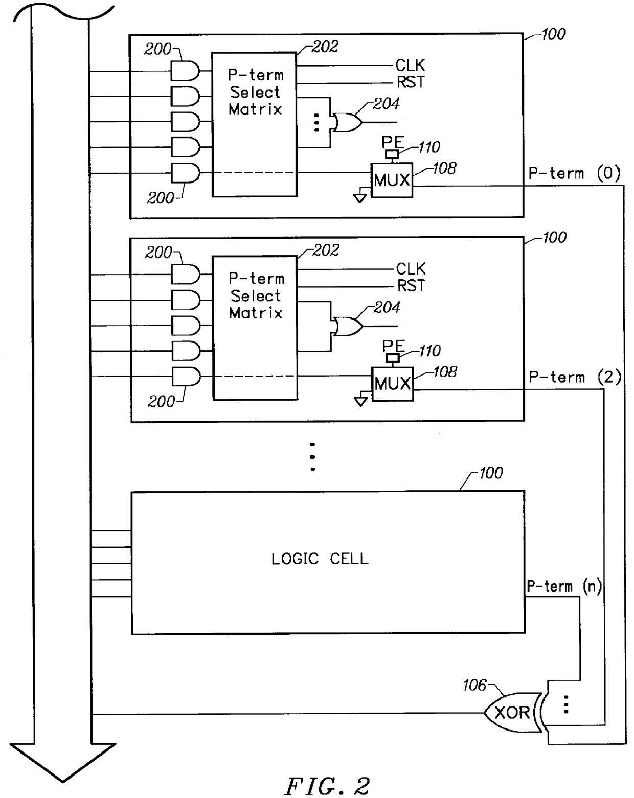
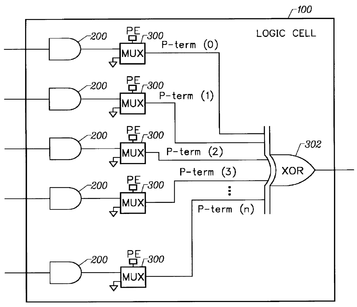
The present invention offers several circuit techniques that provide efficient and fast wide XOR capability for logic cells in p-term based PLDs . In one embodiment, the invention provides a dedicated wide XOR circuit that receives the outputs of a group of logic cells. In another embodiment, a dedicated wide XOR programmably receives multiple p-terms, one from each logic cell in a group of cells. In a third embodiment, a logic cell is provided with an internal XOR gate and multiplexers that allow for programmably cascading several logic cells to implement a wide XOR function. Several other embodiments are also presented that provide variations on the third embodiment with more logic flexibility.
A computer system or other digital processing machine incorporating the invention will benefit from the added flexibility and reprogrammability of the PLD.

Problems solved by technology

This solution uses three logic cells, but is considerably slower since it requires two stages of logic.
Thus, implementing wide XOR with conventional p-term based PLD logic cells is either costly in terms of amount of logic required or slow.
While such devices have met with substantial success, such devices also meet with certain limitations.
This results in an additional level of delay for these logic signals and in use of additional LEs on the PLDs which then can't be used for other functions.

Method used


Image

  • Wide exclusive or and wide-input and for PLDS
  • Wide exclusive or and wide-input and for PLDS
  • Wide exclusive or and wide-input and for PLDS

Examples


Embodiment Construction

Referring to FIG. 1 there is shown a portion of a programmable logic device (PLD) including n logic cells 100 that are grouped into a logic array block (LAB) 102. Such PLD devivces may be, for example, as described in U.S. Pat. Nos. 5,121,006, 5,258,668, 5,260,610, and 5,260,611, all incorporated herein by reference for all purposes. The inputs and outputs of logic cells 100 connect to a programmable interconnect array (PIA) 104. PIA 104 provides programmable interconnection between logic cells 100 inside multiple LABs 102 on a PLD, only one of which is shown in FIG. 1. In this embodiment of the present invention, LAB 102 includes a dedicated XOR 106 with n inputs equal to the number of logic cells 100 inside LAB 102. LAB 102 further includes one select circuit or multiplexer 108 for each input of XOR 106. Each multiplexer 108 has one input connected to a logic cell 100 output, a second input connected to a logic low level (e.g., ground as shown in FIG. 1), a control input connected...


PUM


Abstract

A programmable logic device (10) has a number of programmable logic elements (LES) (12) which are grouped together in a plurality of logic array blocks (LABs) (14). An LAB incorporates one or more wide-input AND gates (74) for selectively combining the outputs of any number of LEs and producing a signal that is a logical combination of any number of its LEs. In variations of the invention, input signals may be selectively coupled to an AND gate by means of an OR gate (78) and may be selectively inverted by means of an XOR gate (76). A digital information processing system (500) incorporating the invention is disclosed. Various circuit techniques are provided for efficient implementation of a fast and wide exclusive OR or exclusive NOR function. A logic array block is equipped with a dedicated exclusive OR circuit with programmable inputs connected to selected terms from various logic cells, or outputs of the various logic cells. Another embodiment allows creating an embedded chain of exclusive OR gates to implement a wide exclusive OR gate by cascading a smaller exclusive OR gate within several logic cells.

Description

BACKGROUND OF THE INVENTIONThe present invention relates generally to programmable logic devices (PLDs), and in particular to various circuit techniques to provide dedicated exclusive OR (XOR) function in complex PLDS.Programmable logic devices are digital, user-configurable integrated circuits used to implement custom logic functions. For the purposes of this description, the term PLD encompasses all digital logic circuits configured by the end-user, including programmable logic arrays (PLAs), field programmable gate arrays (FPGAs), erasable and complex PLDs and the like. Such devices are sometimes referred to as, for example, PALs, FPLAs, EPLDs, EEPLDs, LCAs, CPLDs, and FPGAs. The basic building block of a PLD is the logic cell, sometimes referred to as a macrocell. Typically, a logic cell contains combinatorial logic as well as a programmable flipflop to implement sequential logic. One class of PLDs commonly employs a sum-of-products structure to implement logic functions. In suc...

Claims


Application Information

Patent Timeline
IPC IPC(8): H03K19/177
CPCH03K19/177
Inventor MENDEL, DAVID W.FAIRBANKS, BRENT A.PEDERSEN, BRUCE B.
Owner ALTERA CORP
Learn More