Voltage level shifter

Inactive Publication Date: 2000-03-28
ARM LTD
View PDF6 Cites 63 Cited by
  • Summary
  • Abstract
  • Description
  • Claims
  • Application Information

AI Technical Summary

Problems solved by technology

As a result the desired output of "0" is not reliably produced since the transition voltages of the transistors 4,6 may not be adequately cleared by the input signal level.
This dc current flow is a severe disadvantage since it wastes a considerable amount of power.
However, the problem of the dc current path still persists and is a severe disadvantage.
If each of these interface circuits wastes power through the above dc current, then the total power loss is significant.
For the duration of the transition and latching operation there will be such a dependence that can suffer from the problem that the low voltage signals cannot fully switch

Method used


Image

  • Voltage level shifter
  • Voltage level shifter
  • Voltage level shifter

Examples


Embodiment Construction

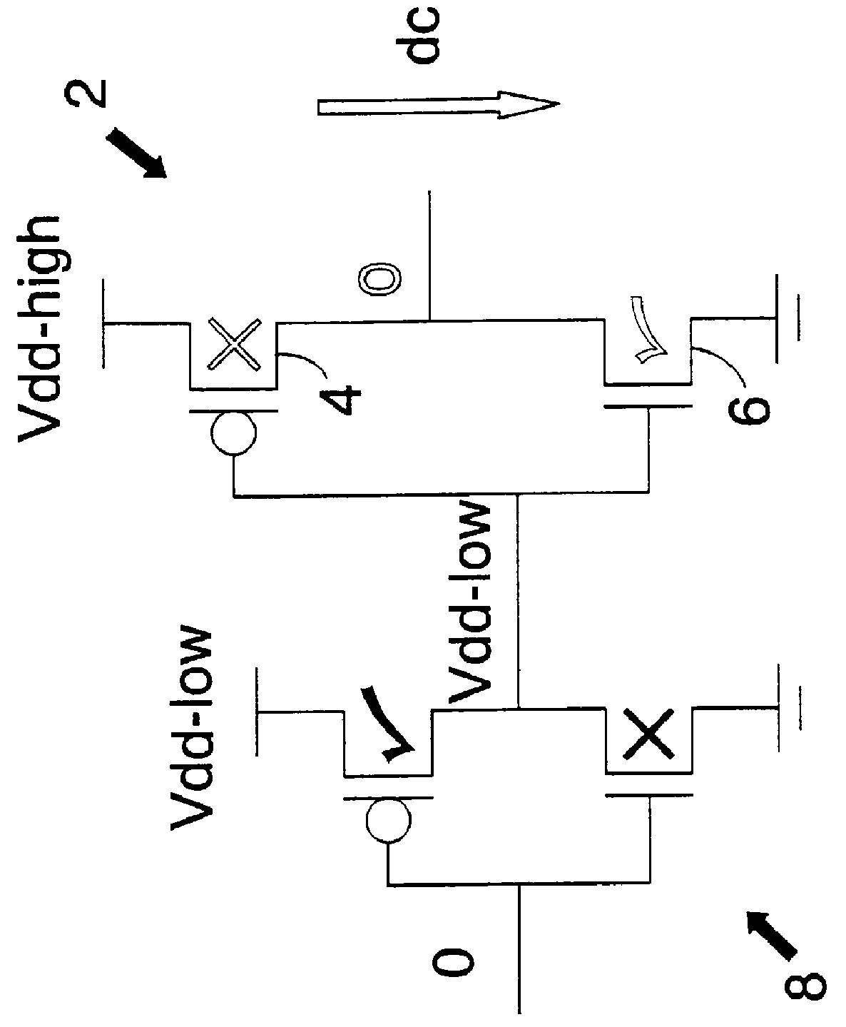
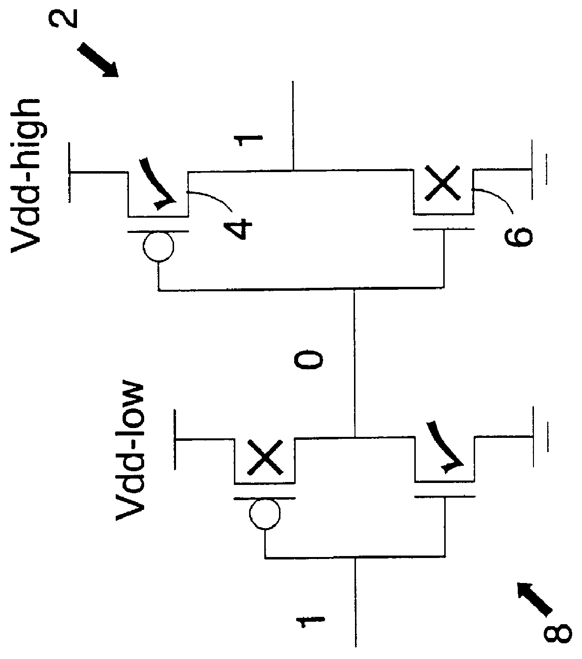
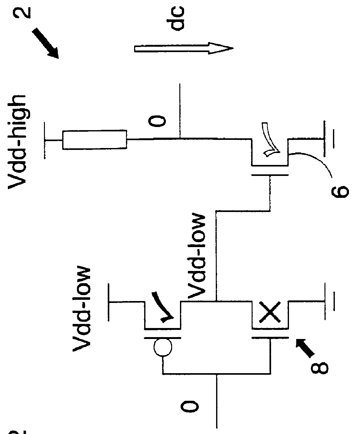
FIG. 3 shows a digital circuit having a low voltage portion 12 and a high voltage portion 14. A low voltage digital signal on the input line 16 needs to be passed from the low voltage portion 12 to the high voltage portion 14. An edge detector circuit 18 (which can have several known forms) serves to generate a pulse signal giving a temporary "0-1-0" output in response to either a rising edge or a falling edge in the signal of the input line 16.

The interface circuit 20 includes a resistor element 22, a switching transistor 24 and a sensing transistor 26 all connected in series between the high supply voltage Vdd-high and ground (it will be appreciated that the transitors could be in a different order without altering the basic operation of the system). The output from the edge detector 18 serves to temporarily switch on the switching transistor 24 whenever a transition is detected on the input line 16. When the switching transistor 24 is switched on, the output from the sensing tran...


PUM


Abstract

The present invention provides a voltage level shifter for use in a digital circuit having a low voltage portion and a high voltage portion. The voltage shifter comprises an interface circuit 20,32,60 that senses transitions in a low voltage digital signal from an old value to a new value and uses these to trigger latching of the new value. The latch can be a SR latch 34,62 with its set 40 and reset 42 inputs coupled to pulse generators 46,68,58,70 respectively responsive to rising and falling edges in the input low voltage signal being passed from the low voltage portion to the high voltage portion. Feedback from the output on the latch 62 can be controlled to limit the duration of the pulses from the pulse generators 68,70 and thereby reduce power consumption due to the dc current leakage associated with a low voltage to high voltage signal interface.

Description

1. Field of the InventionThe present invention relates to digital circuits. More particularly, the present invention relates to digital circuits having a low voltage portion and a high voltage portion between which it is desired to pass digital signals.2. Description of the Prior ArtIt is known in the field of digital circuits to provide digital circuits with an interface circuit between a low voltage portion and a high voltage portion. FIGS. 1A, 1B, 2A and 2B of the accompanying drawings show examples of such interface circuits.FIGS. 1A and 1B show an example of an interface circuit taking the simple form of an invertor 2 composed of a p-type transistor 4 and an n-type transistor 6. The signal from the low voltage portion is first passed to a buffer in the form of an invertor 8 that serves to ensure the digital signal being passed to the high voltage portion is either at the ground voltage level or at the low voltage supply level Vdd-low. When the digital signal input to the transi...

Claims


Application Information

Patent Timeline
IPC IPC(8): H03K19/0185
CPCH03K19/018507
Inventor HILL, STEPHEN JOHN
Owner ARM LTD
Why Eureka
Try Eureka