Light emitting artwork
a technology of light-emitting artwork and light-emitting devices, applied in the field of art, can solve problems such as being unsuitable for purposes
- Summary
- Abstract
- Description
- Claims
- Application Information
AI Technical Summary
Problems solved by technology
Method used
Image

Examples
first embodiment
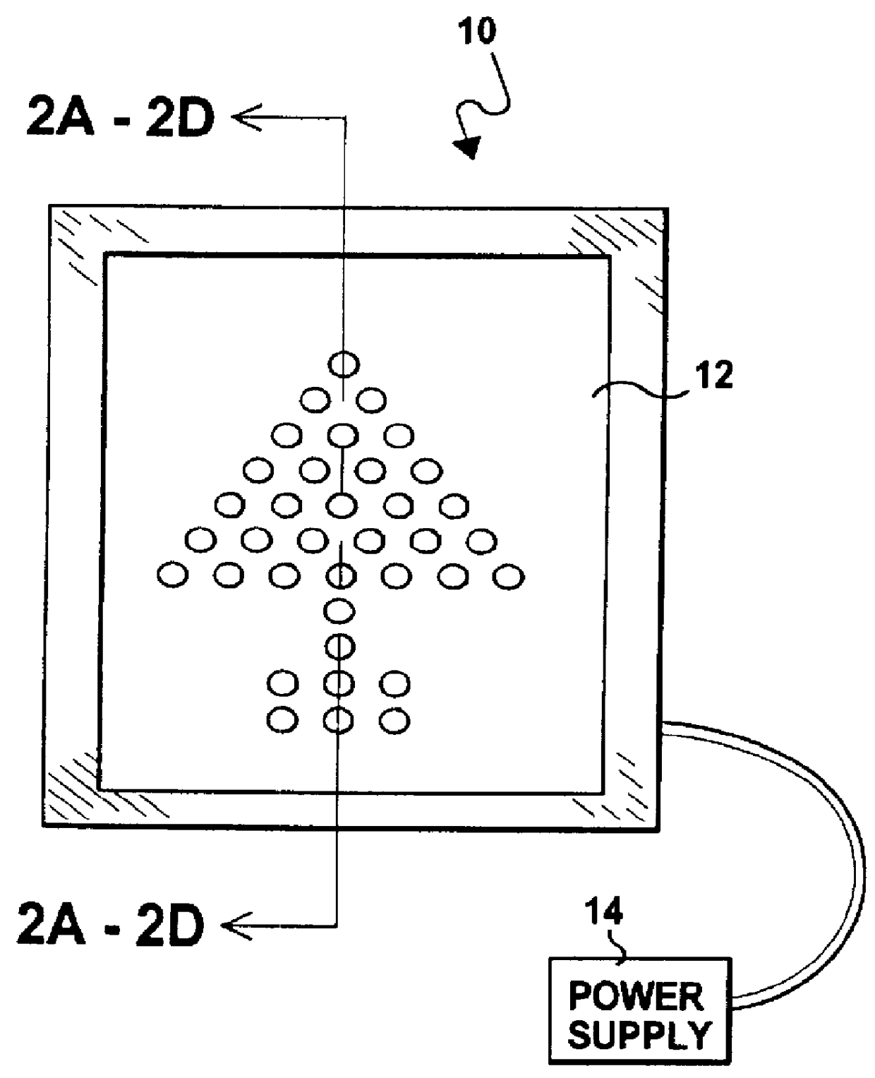
The configuration of the light emitting artwork 10 can best be seen in FIG. 2A, and as such as will be discussed with reference thereto.
The light emitting artwork 10 includes a printed circuit board 16 that is preferably epoxy glass and has a front surface 18 and a back surface 20 with metal lands 22 thereon that have a back surface 24.
Alternatively, the light emitting artwork 10 may include an insulated sheet material 16 that has a front surface 18 and a back surface 20 with metal conductors 22 that connect components mounted thereon or therethrough, with the metal connectors 22 being at least one of wire and foil.
The light emitting artwork 10 further includes at least one Light Emitting Device the acronym for which is LED 26 positioned directly on the front surface 18 of the printed circuit board 16, at any desirable location for providing customized light emitting artwork.
The at least one LED 26 has leads 28 that pass through the printed circuit board 16 which are soldered to the...
second embodiment
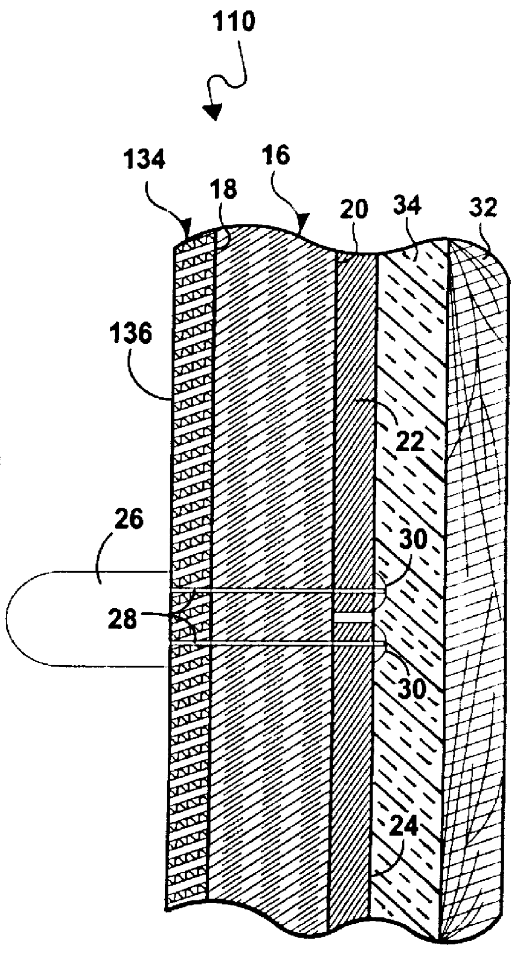
The configuration of the light emitting artwork 110 can best be seen in FIG. 2B, and as such will be discussed with reference thereto.
The light emitting artwork 110 is similar to the light emitting artwork 10, with the addition of a surface material 134 mounted directly onto the front face 18 of the printed circuit board 16. The surface material 134 has an exposed front surface 136 with an optional image thereon that together with the at least one LED 26, if present, produce the customized light emitting artwork.
The at least one LED 26, however, is positioned directly on the exposed front surface 136 of the surface material 134, at any desirable location, instead of directly on the front surface 18 of the printed circuit board 16, as in the light emitting artwork 10.
The leads 28 of the at least one LED 26 pass through the surface material 134, through the printed circuit board 16, and are soldered to the back surface 24 of the metal lands 22 on the back surface 20 of the printed cir...
third embodiment
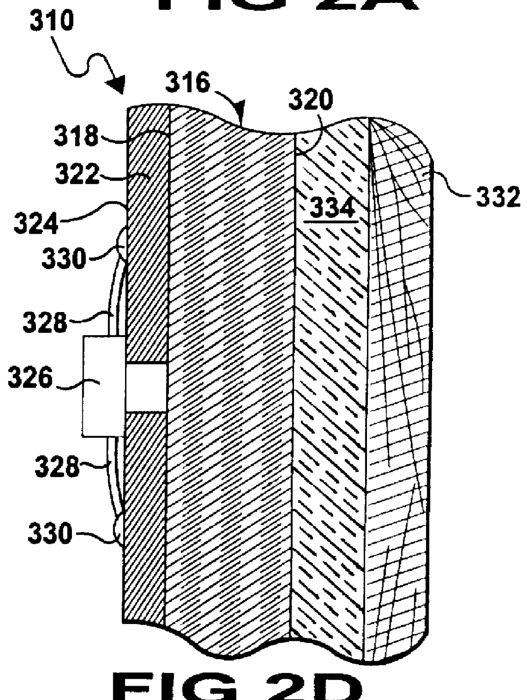
The configuration of the light emitting artwork 210 can best be seen in FIG. 2C, and as such will be discussed with reference thereto.
The light emitting artwork 210 is similar to the light emitting artwork 110, except that the at least one LED 26 is positioned directly on the front surface 18 of the printed circuit board 16, as in the light emitting artwork 10, but sitting in and visible from an aperture 238 in the surface material 134, with the surface material 134 abutting directly against the sides of the at least one LED 26.
PUM
 Abstract
Description
Claims
Application Information
 - Generate Ideas
- Intellectual Property
- Life Sciences
- Materials
- Tech Scout
- Unparalleled Data Quality
- Higher Quality Content
- 60% Fewer Hallucinations
Browse by: Latest US Patents, China's latest patents, Technical Efficacy Thesaurus, Application Domain, Technology Topic, Popular Technical Reports.
© 2025 PatSnap. All rights reserved.Legal|Privacy policy|Modern Slavery Act Transparency Statement|Sitemap|About US| Contact US: help@patsnap.com