Current constricting phase change memory element structure

a phase change memory and current constricting technology, applied in the field of semiconductor structures, can solve the problems of significant variations in the resistance of the mixed phase change material layer, the difficulty of increasing the density of the pcm device, etc., and achieve the effect of reducing the size of the programming transistor

Inactive Publication Date: 2009-01-15
MACRONIX INT CO LTD +2
View PDF5 Cites 113 Cited by
  • Summary
  • Abstract
  • Description
  • Claims
  • Application Information

AI Technical Summary

Benefits of technology

[0012]Specifically, a layer of nanoparticles having a dimension on the order of about 10 nm is employed to form a current constricting layer or as a hardmask for forming a current constricting layer from an underlying insulator layer. The nanoparticles are preferably self-aligning and/or self-planarizing on the underlying surface. The current constricting layer may be formed within a bottom conductive plate, within a phase change material layer, within a top conductive plate, or within a tapered liner between a tapered via sidewall and a via plug contain

Problems solved by technology

One of the challenges of present day PCM element structures is to generate sufficient heat to reach the melting temperature of the phase change material.
However, application of such a large current requires a large transistor, and consequently a large semiconductor area, making it difficult to increase the density of PCM device

Method used


Image

  • Current constricting phase change memory element structure
  • Current constricting phase change memory element structure
  • Current constricting phase change memory element structure

Examples


first embodiment

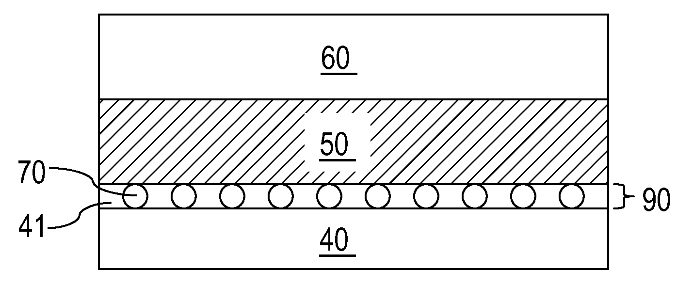
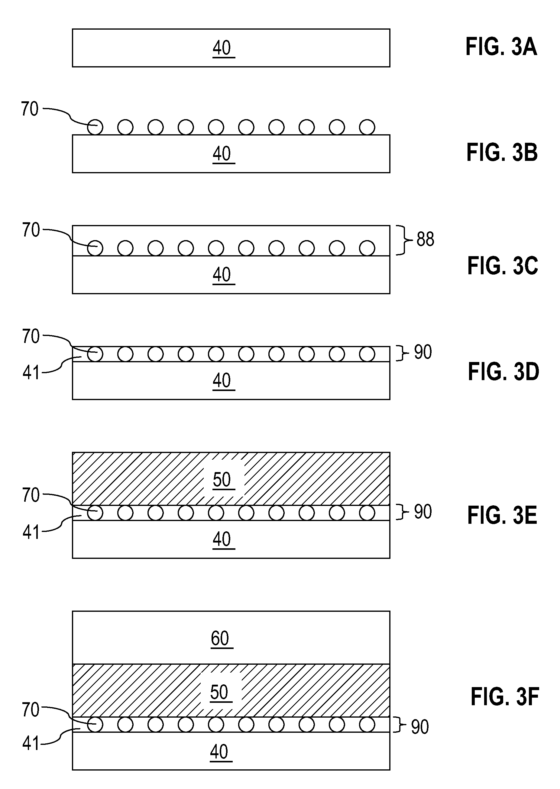
[0052]Sequential cross-sectional views of a first exemplary structure according to the present invention are shown at various stages of a manufacturing process in FIGS. 3A-3F. Referring to FIG. 3A, a bottom conductive plate 40 is formed on an underlying semiconductor structure (not shown). The bottom conductive plate 40 may be formed by chemical vapor deposition or sputtering of a metal layer. Methods of placing the bottom conductive plate 40 in a semiconductor structure for the purpose of forming a PCM memory element is well known in the art. The bottom conductive plate 40 comprises a conductive material that may be, for example, selected from Ti, Ta, W, Mo, Al, Cu, Pt, Ir, La, Ni, Ru, another elemental metal, and alloys thereof. The thickness of the bottom conductive plate 40 is typically in the range from about 10 nm to about 80 nm.

[0053]Referring to FIG. 3B, a monolayer of insulating nanoparticles 70 is applied to a top surface of the bottom conductive plate 40. Each of the insu...

third embodiment

[0074]Referring to FIG. 6C, an insulating layer 80 is formed on the first phase change material layer 51, for example, by chemical vapor deposition. The insulating layer 80 is formed by the same method as and comprises the same material as the insulating layer 80 according to the The thickness of the insulating layer 80 may be from about 3 nm to about 60 nm.

[0075]Referring to FIG. 6D, a monolayer of insulating nanoparticles 70 is applied to a top surface of the insulating layer 80. The same type of insulating nanoparticles 70 may be employed as in the first embodiment. Preferably, the insulating nanoparticles 70 are self-aligning and / or self-planarizing on the top surface of the insulating layer 80. The monolayer of insulating nanoparticles 70 are separated among one another so that gaps are present among the insulating nanoparticles 70 when viewed from above. The gaps may be contiguous or many be disjoined among one another.

[0076]Referring to FIG. 6E, an anisotropic reactive ion e...

seventh embodiment

[0096]Referring to FIG. 9, a seventh exemplary structure according to the present invention comprises a bottom conductive plate 40, a phase change material layer 50, a dielectric layer 77 containing a tapered via hole sidewall 78, a tapered via liner 110 having a liner bottom surface 79, and a conductive via plug 60′. The phase change material layer 50 abuts the bottom conductive plate 40 located underneath, the liner bottom surface 79, and the dielectric layer 77. The tapered via liner 110 abuts the tapered via hole sidewall 78 and contains a monolayer of insulating nanoparticles 70 that are embedded in and separated by a volume 65 of a conductive material. The conductive via plug 60′ comprises the same conducive material as the volume 65 of the conductive material within the tapered via liner 110.

[0097]The bottom conductive plate 40 and the conductive via plug 60′ comprise a conductive material that may be, for example, a material selected from Ti, Ta, W, Mo, Al, Cu, Pt, Ir, La, N...


PUM


Abstract

A layer of nanopaiticles having a dimension on the order of 10 nm is employed to form a current constricting layer or as a hardmask for forming a current constricting layer from an underlying insulator layer. The nanoparticles are preferably self-aligning and/or self-planarizing on the underlying surface. The current constricting layer may be formed within a bottom conductive plate, within a phase change material layer, within a top conductive plate, or within a tapered liner between a tapered via sidewall and a via plug contains either a phase change material or a top conductive material. The current density of the local structure around the current constricting layer is higher than the surrounding area, thus allowing local temperature to rise higher than surrounding material. The total current required to program the phase change memory device, and consequently the size of a programming transistor, is reduced due to the current constricting layer.

Description

FIELD OF THE INVENTION[0001]The present invention relates to semiconductor structures, and particularly to phase change memory element structures having a current constricting layer and methods of manufacturing the same.BACKGROUND OF THE INVENTION[0002]A phase change memory (PCM) device is a non-volatile memory device employing a change in resistivity of a phase change material. The PCM device is also called phase-change random access memory (PRAM). Typically, a chalcogenide material capable of switching between an amorphous state and a crystalline state is employed in PCM devices.[0003]Depending on the cooling rate from a liquid state, the chalcogenide material may form an amorphous chalcogenide glass or a chalcogenide crystal. The difference between the two states is physically characterized by the presence or absence of a long range order. Further, the crystalline and amorphous states of chalcogenide material have drastically different resistivity values. By manipulating the phas...

Claims


Application Information

Patent Timeline
IPC IPC(8): H01L29/04
CPCB82Y10/00H01L45/06H01L45/1233H01L45/1246H01L45/16H01L45/143H01L45/144H01L45/148H01L45/1273H10N70/828H10N70/8418H10N70/8825H10N70/884H10N70/231H10N70/011H10N70/8828H10N70/826
Inventor CHEN, CHIEH-FANGCHEN, SHIH HUNGCHEN, YI-CHOUHAPP, THOMASHO, CHIA HUAHSUEH, MING-HSIANGLAM, CHUNG HONLUNG, HSIANG-LANPHILIPP, JAN BORISRAOUX, SIMONE
Owner MACRONIX INT CO LTD
Why Eureka
Try Eureka