

Method for forming a self-aligned copper structure with improved planarity
- Summary
- Abstract
- Description
- Claims
- Application Information
AI Technical Summary
Benefits of technology
Problems solved by technology
Method used
Image

Examples
Embodiment Construction
--FIGS. 3 through 6
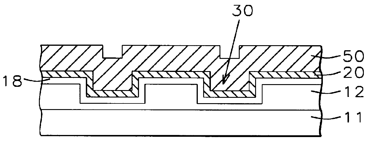
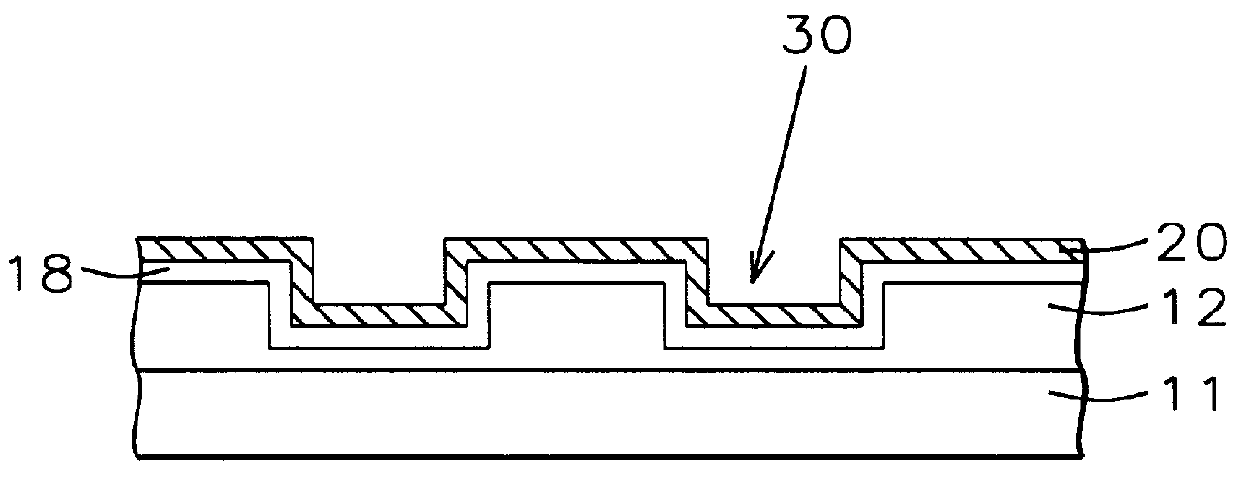
Referring to FIG. 3, the preferred embodiment of the present invention begins by providing a semiconductor structure (11) having a dielectric layer (12) thereover, wherein one or more trenches (30) are formed in the dielectric layer, as in the problem process. The trenches (30) can extend all the way through the dielectric layer (12) to expose a conductive area (e.g. another conductive line or a doped area of an underlying substrate). The dielectric layer can be an inter level dielectric (ILD) or an inter metal dielectric (IMD).
As in the problem process, a barrier layer (18) is formed over the dielectric trench layer (12), and a seed layer (20) is formed on the barrier layer (18). The barrier layer (18) is preferably composed of tantalum nitride having a thickness of between about 50 Angstroms and 600 Angstroms. The seed layer (20) preferably is comprised of seed copper having a thickness of between about 1000 Angstroms and 3000 Angstroms. The seed layer can be co...
PUM
 Abstract
Description
Claims
Application Information