Integrated circuit with field programmable and application specific logic areas

Inactive Publication Date: 2000-07-25
XILINX INC
View PDF9 Cites 186 Cited by
  • Summary
  • Abstract
  • Description
  • Claims
  • Application Information

AI Technical Summary

Benefits of technology

It is another object of the invention to provide a combined FPGA/ASLA on a single mono

Problems solved by technology

The total cost of the chip at such a point in its life cycle tends to be greater when the chip is a field programmable IC rather than a mask-defined chip.
One reason field programmable chips ha

Method used


Image

  • Integrated circuit with field programmable and application specific logic areas
  • Integrated circuit with field programmable and application specific logic areas
  • Integrated circuit with field programmable and application specific logic areas

Examples


Embodiment Construction

The following description constitutes a disclosure of the best mode of the invention presently contemplated by the inventors. It is intended to be merely illustrative of an integrated circuit architecture embodying the invention without limiting the scope of protection afforded by applicable patent law.

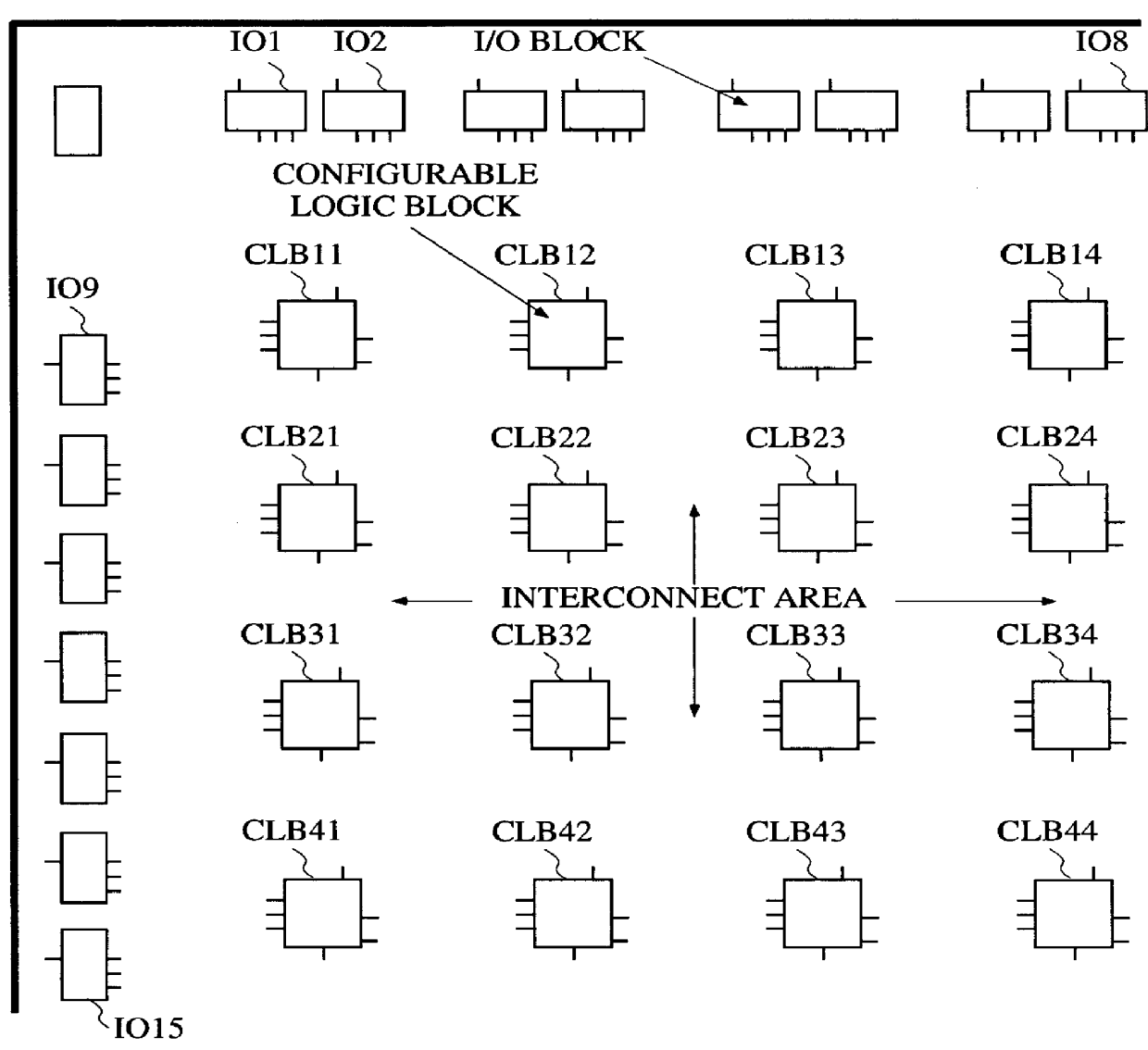
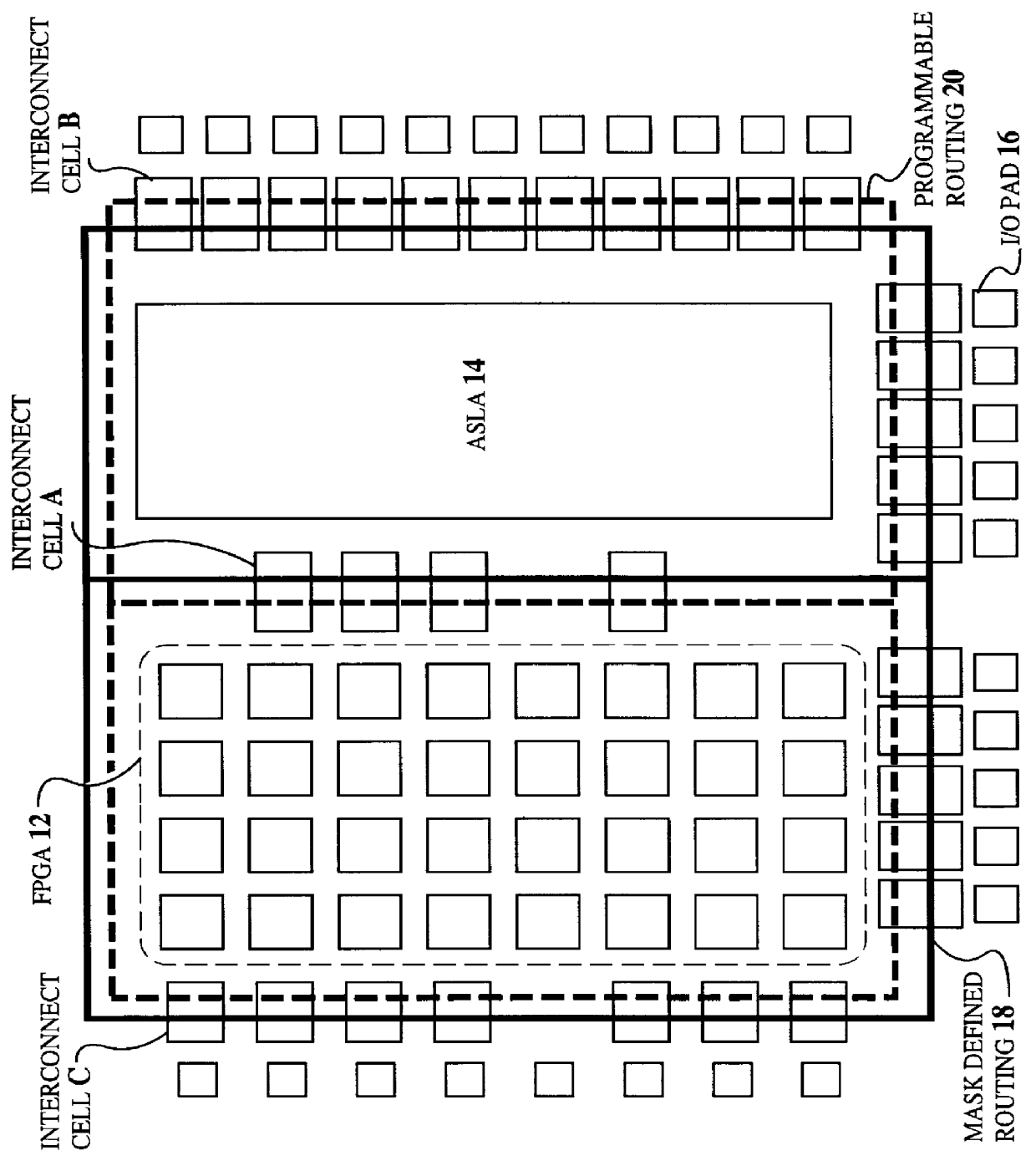
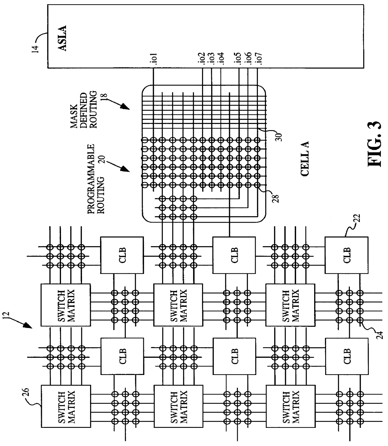
Referring first to FIG. 2, it will be seen that the preferred embodiment of a monolithic circuit device 10 in accordance with the present invention comprises an FPGA portion 12 or array of programmable gates and an ASLA portion 14 or array of mask-defined gates. Device 10 also comprises a plurality of input / output (I / O) pads 16 providing externally accessible signal connections to the respective arrays 12 and 14. ASLA 14 may comprise a hard-wired version of an earlier FPGA such as described by Buch et al. in U.S. Pat. No. 5,550,839, may comprise a standard cell array with customized metal layers such as manufactured by LSI Logic, Inc., or may comprise a custom logic device in which al...


PUM


Abstract

A heterogeneous integrated circuit device comprising a field programmable gate array (FPGA) programmably connected to a mask-defined application specific logic area (ASLA) on an integrated circuit thus providing a flexible low cost alternative to a homogeneous device of one type or the other. By integrating both on a single monolithic IC, the user benefits from both low cost and flexibility. Routing of signals between gate arrays and between the gate arrays and input/output (I/O) circuits is also implemented as a combination of mask-defined and programmably-configured interconnections.

Description

This invention relates to a structure and method for performing custom logic functions in an integrated circuit logic device.DESCRIPTION OF THE BACKGROUND ARTAdvancements in the technology of integrated circuits have enabled designers to place relatively large numbers of digital logic gates as an array on a single integrated circuit chip (IC). Numerous approaches have evolved for interconnecting the logic gates of such high density, digital logic ICs.A first approach, which may be described by terms such as hard-wired interconnection, metal interconnection, etc. and is referred to herein as mask-defined, uses the fixed layout of various conductive paths in the IC that are either diffused in the substrate or patterned in metallization layers of the IC to interconnect input and output terminals of logic gates, one to the next. As integrated circuit devices have become able to perform more functions within a single integrated circuit chip, the manufacturers of integrated circuit chips ...

Claims


Application Information

Patent Timeline
IPC IPC(8): H03K19/177G06F15/78
CPCG06F15/7867H03K19/17704H03K19/17796
Inventor TAVANA, DANESHYEE, WILSON K.TRIMBERGER, STEPHEN M.
Owner XILINX INC
Why Eureka
Try Eureka