Semiconductor device testing apparatus

a technology of semiconductor devices and testing apparatuses, which is applied in the direction of individual semiconductor device testing, semiconductor/solid-state device testing/measurement, instruments, etc., can solve the problems of large waste in the floor space, inability to successfully deposit ics into ic storage recesses, and significant limitation of the number of ic testing apparatus that can be installed

Inactive Publication Date: 2000-08-15
ADVANTEST CORP
View PDF4 Cites 62 Cited by
  • Summary
  • Abstract
  • Description
  • Claims
  • Application Information

AI Technical Summary

Problems solved by technology

Consequently, if the ICs as such were vacuum picked up by the suction pads and transferred directly to the test tray TST, there might be some of the ICs which could not be successfully deposited into the IC storage recesses formed in the test tray TST.
As a result, where numerous IC testing apparatuses are installed, there would be much waste in the floor space and the number of IC testing apparatus that can be installed would be significantly limited.
In addition, with the IC testing apparatus according to the fifth aspect, since the sorting operation is carried out with respect to only the general-purpose trays arranged adjacent to each of the unloader sections, the sorting speed is increased, resulting in speeding up the entire testing process.

Method used


Image

  • Semiconductor device testing apparatus
  • Semiconductor device testing apparatus
  • Semiconductor device testing apparatus

Examples


first embodiment

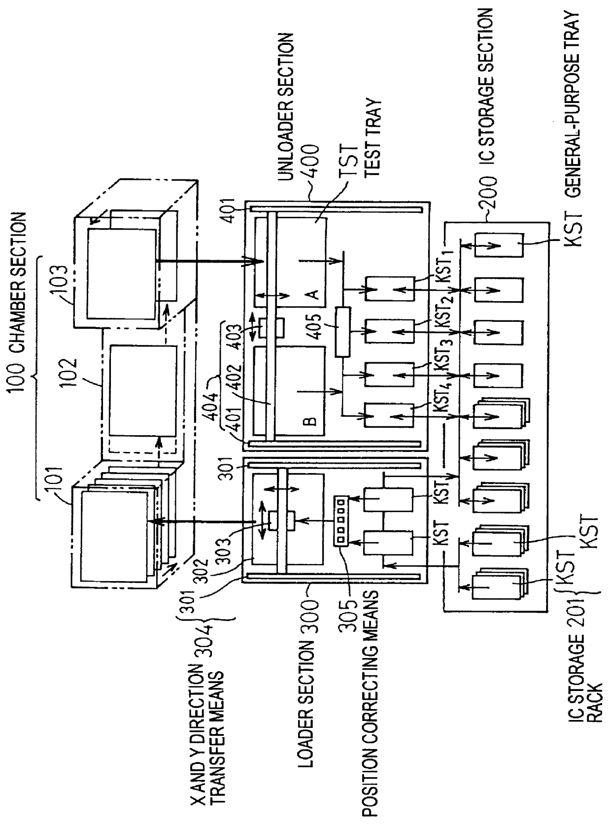
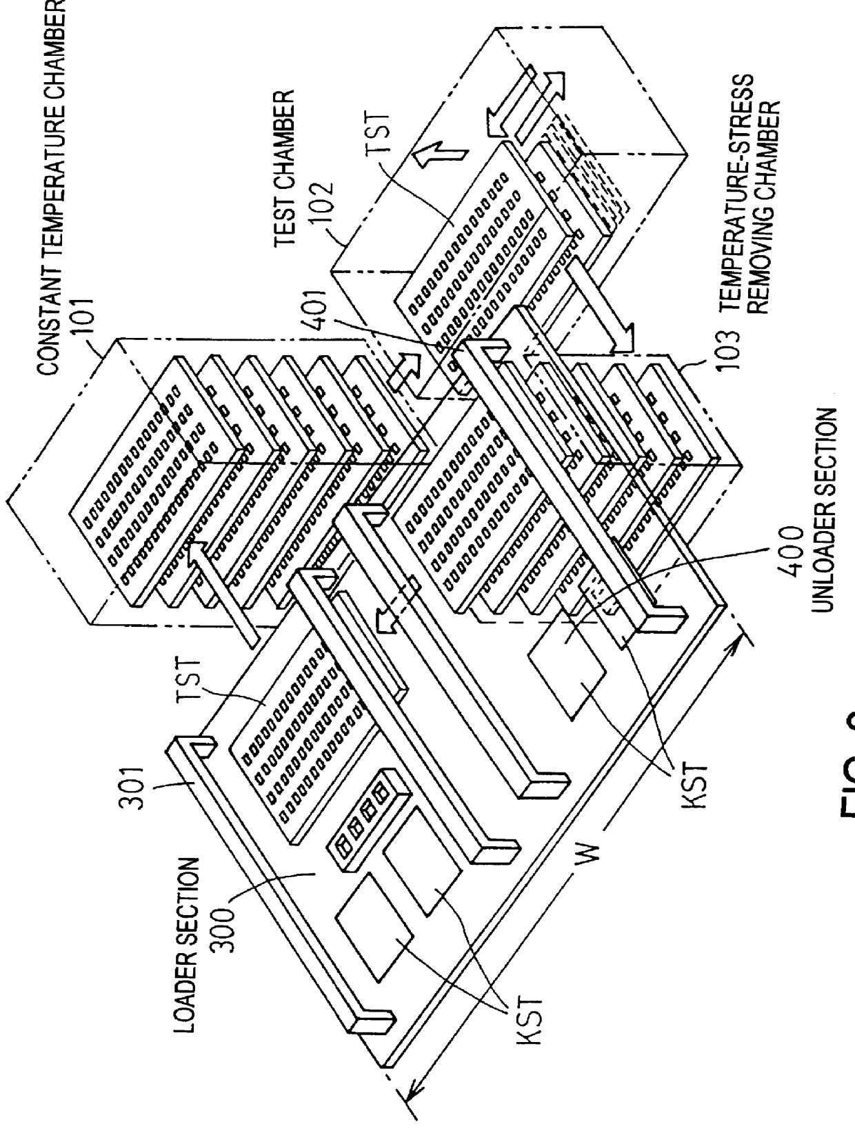
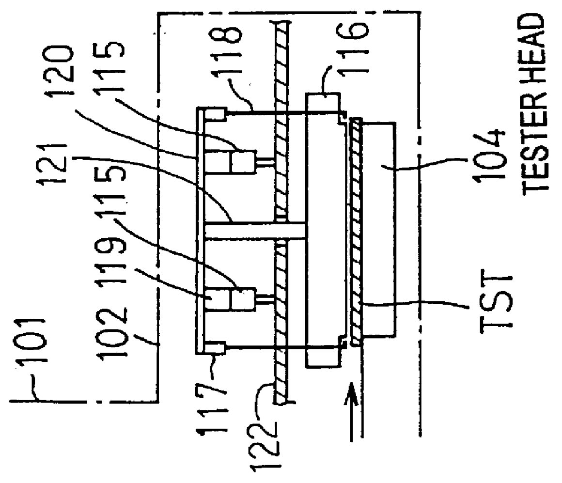
FIG. 1 shows the IC testing apparatus according to the present invention. The elements or parts shown in FIG. 1 corresponding to those of FIG. 4 are designated by the same reference numerals and will not be discussed again in detail, unless required. As with the conventional example shown in FIG. 4, the IC testing apparatus of the present invention comprises a chamber section 100, an IC storage section 200 for storing ICs to be tested and ICs already tested and sorted, a loader section 300 where ICs to be tested which a user has beforehand loaded on general-purpose trays KST are transferred and reloaded onto a test tray TST capable of withstanding high / low temperatures, and an unloader section 400 where the tested ICs which have been carried on the test tray TST out of the chamber section 100 subsequently to undergoing a test therein are transferred from the test tray TST to the general-purpose trays KST to be reloaded on the latter. The chamber section 100 comprises a constant temp...

second embodiment

According to the IC testing apparatus of the second embodiment, it is possible to reduce the transverse width W of the handler portion to about two test tray lengths, since it is only the constant temperature chamber 101 and the test chamber 102 that are arranged transversely of the IC testing apparatus (although the loader section 300 and the unloader section 400 are also transversely arranged, they are located either in front of or in the rear of the constant temperature chamber 101 and the test chamber 102). As a result, an IC testing apparatus with a further reduced transverse width may be provided.

In addition, with the testing apparatus according to the present invention, it is possible to adopt the arrangement in which a common X and Y direction transfer means 404 is disposed with respect to an unloader section 400 having two stop positions A and B for a test tray, enabling the reduction by one of the number of X and Y direction transfer means required and hence leading to red...


PUM


Abstract

PCT No. PCT/JP96/02067 Sec. 371 Date May 28, 1997 Sec. 102(e) Date May 28, 1997 PCT Filed Jul. 24, 1996 PCT Pub. No. WO97/05495 PCT Pub. Date Feb. 13, 1997A semiconductor device testing apparatus having a reduced transverse width and compact in size is provided. Adjacent to a constant temperature chamber 101 containing therein a vertical transport means is located a test chamber 102 which is in turn adjoined by a temperature-stress removing chamber 103 likewise containing therein a vertical transport means, so that the constant temperature chamber 101, the test chamber 102 and the temperature-stress removing chamber 103 are arranged transversely in a line. Further, a loader section 300 is located in front of the constant temperature chamber, and an unloader section 400 is located in front of the test chamber and the temperature-stress removing chamber. With this arrangement, the transverse width of the testing apparatus may be reduced to about three test tray lengths.

Description

1. Field of the InventionThe present invention relates to a semiconductor device testing apparatus suitable for testing one or more semiconductor devices, particularly one or more semiconductor integrated circuit elements (as will be referred to as IC or ICs hereinafter) which are typical examples of the semiconductor devices. More particularly, the present invention relates to a semiconductor device testing apparatus of the type in which ICs to be tested are transported, for testing, to a test or testing section where they are brought into electrical contact with a tester head (a component of the testing apparatus for applying and receiving various electrical signals for testing), followed by being carried out of the testing section and then being sorted out into conformable or pass articles and unconformable or failure articles on the basis of the test results.2. Background of the Related ArtMany of the semiconductor device testing apparatuses (commonly called IC testers) for appl...

Claims


Application Information

Patent Timeline
Patent Type & Authority Patents(United States)
IPC IPC(8): G01R31/28G01R31/26H01L21/677
CPCG01R31/2868G01R31/26H01L22/00
Inventor KOBAYASHI, YOSHIHITOYAMASHITA, TSUYOSHINAKAMURA, HIROTONEMOTO, SHINMASUO, YOSHIYUKIITO, AKIHIKO
Owner ADVANTEST CORP
Why Eureka
Try Eureka