Method and apparatus for controlling semiconductor wafer fabrication equipment based on a remaining process time applicable to the processors

a technology of semiconductor wafers and processing equipment, applied in the direction of program control, total factory control, furnaces, etc., can solve the problems of increasing idle time, reducing the availability of processors correspondingly, and affecting the processing of cassettes that are urgently desired to be processed,

Inactive Publication Date: 2000-10-17
MITSUBISHI ELECTRIC CORP
View PDF8 Cites 115 Cited by
  • Summary
  • Abstract
  • Description
  • Claims
  • Application Information

AI Technical Summary

Problems solved by technology

The growing idle time lowers the availability of the processors correspondingly.
However, to select one at a time those cassettes stored in all stockers still requires solving the problem of how to minimize the idle time of the processors in connection with the transport task scheduling described above.
The procedure tends to overload the transport means.
Furthermore, because the cassettes held in the overflow stocker are always given priority when processed, the processing of those cassettes desired to be processed urgently tends be delayed.

Method used


Image

  • Method and apparatus for controlling semiconductor wafer fabrication equipment based on a remaining process time applicable to the processors
  • Method and apparatus for controlling semiconductor wafer fabrication equipment based on a remaining process time applicable to the processors
  • Method and apparatus for controlling semiconductor wafer fabrication equipment based on a remaining process time applicable to the processors

Examples


first embodiment

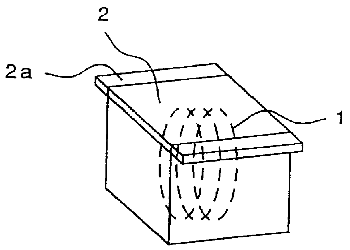
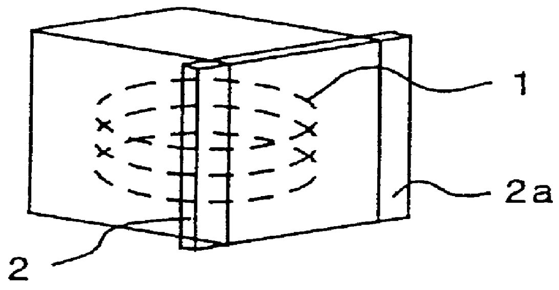
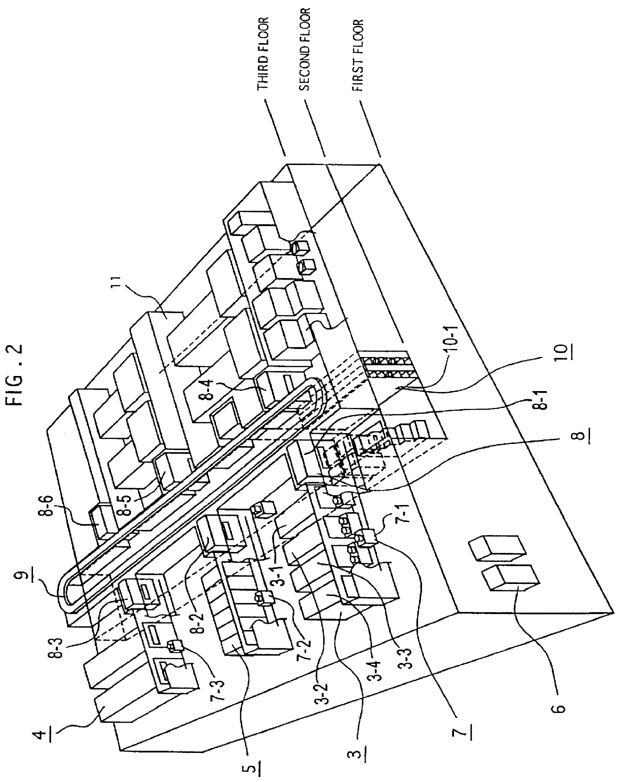
In a first embodiment of the present invention, semiconductor wafers 1, cassettes 2, and semiconductor fabrication equipment are basically the same in structure as their conventional counterparts described earlier with reference to FIGS. 1 through 10. One difference that characterizes the first embodiment concerns the bay stocker 8 whose operation was described above in connection with FIG. 6. In the conventional example, there is no direct transport of cassettes 2 between the OHS port 8e and the AGV port 8d by the stocker crane 8b. Each cassette 2 coming from either of these ports is always stored into the stocker shelves 8c. With the first embodiment, by contrast, cassettes are transported directly between the OHS port 8e and the AGV port 8d.

The transport control method of the inventive semiconductor fabrication equipment will now be described in detail. Five major subjects will be discussed: (1) an automatic control program for the processor (A), (2) an automatic control program ...


PUM


Abstract

Semiconductor wafer fabrication equipment comprising a selecting device for selecting semiconductor wafers destined to a processor on the basis of a remaining process time applicable to that processor in the equipment, a transporting device for transporting the selected semiconductor wafers to the processor, another selecting device for selecting a processor or a storage device constituting a transport destination to which to transport processed semiconductor wafers, and another transporting device for transporting the semiconductor wafers to the destination processor or storage device in accordance with a transport control changeover code read from the processors and storage devices of the equipment.

Description

1. Field of the InventionThe present invention relates to a method for controlling the transport of semiconductor wafer carriers used by equipment for fabricating semiconductor integrated circuits.2. Background ArtFIGS. 1A and 1B are perspective views showing a cassette containing semiconductor wafers. In the figures, reference numeral 1 represents semiconductor wafers (simply called wafers hereunder) from which numerous semiconductor integrated circuits (not shown) are produced. Reference numeral 2 denotes a semiconductor wafer cassette (simply called the cassette hereunder) that serves as a transport unit carrying a plurality of wafers 1. FIG. 1A sketches a horizontally positioned cassette 2 in which the wafers 1 are positioned perpendicularly, with a wafer removal side 2a facing up. FIG. 1B portrays a vertically positioned cassette 2 wherein the wafers 1 are positioned horizontally, with the wafer removal side 2a facing sideways.FIG. 2 is a perspective view of typical semiconduct...

Claims


Application Information

Patent Timeline
Patent Type & Authority Patents(United States)
IPC IPC(8): G05B19/418H01L21/00B65G47/50B65G43/08B65G49/07H01L21/02H01L21/677
CPCG05B19/41865H01L21/67769H01L21/67276G05B2219/32266G05B2219/45031G05B2219/32319Y02P90/02
Inventor IWASAKI, JUNJI
Owner MITSUBISHI ELECTRIC CORP
Why Eureka
Try Eureka