Electrical critical dimension measurement and defect detection for reticle fabrication

Inactive Publication Date: 2005-12-06
GLOBALFOUNDRIES INC
View PDF14 Cites 19 Cited by
  • Summary
  • Abstract
  • Description
  • Claims
  • Application Information

AI Technical Summary

Benefits of technology

[0008]The following presents a simplified summary of the invention in order to provide a basic understanding of some aspects of the invention. This summary is not an extensive overview of the invention. It is intended to neither identify key or critical elements of the invention nor delineate the scope of the invention. Its sole purpose is to present some concepts of the invention in a simplified form as a prelude to the more detailed description that is presented later.
[0009]A system and method are provided to determine critical dimensions and to detect defects in a reticle for semiconductor processing. In one embodiment, the system and method employ test structures for electrical resistance measurements of metal lines fabricated in the metal or opaque layer of a reticle. To avoid wasting space, test structures are located within the scribe lines between the multiple device feature areas of the reticle. The device feature area is the area of the reticle where the features of the integrated circuits are located. Multiple device feature areas are separated by scribe lines. When space allows, the test structure can be located within the actual device feature area. The test structures may also be located within both the scribe lines and within the actual device feature layout. The test structures contain test features constructed to replicate the critical dimensions of the device feature

Problems solved by technology

While visual inspection techniques may be simple to implement, they are difficult to automate, and furthermore, have typically operated in isolation from other fabricati

Method used


Image

  • Electrical critical dimension measurement and defect detection for reticle fabrication
  • Electrical critical dimension measurement and defect detection for reticle fabrication
  • Electrical critical dimension measurement and defect detection for reticle fabrication

Examples


Embodiment Construction

[0032]The present invention will now be described with reference to the drawings wherein like reference numerals are used to refer to like elements throughout. The following detailed description is of the best mode presently contemplated by the inventors for practicing the invention. It should be understood that the description of these aspects are merely illustrative and that they should not be taken in a limiting sense.

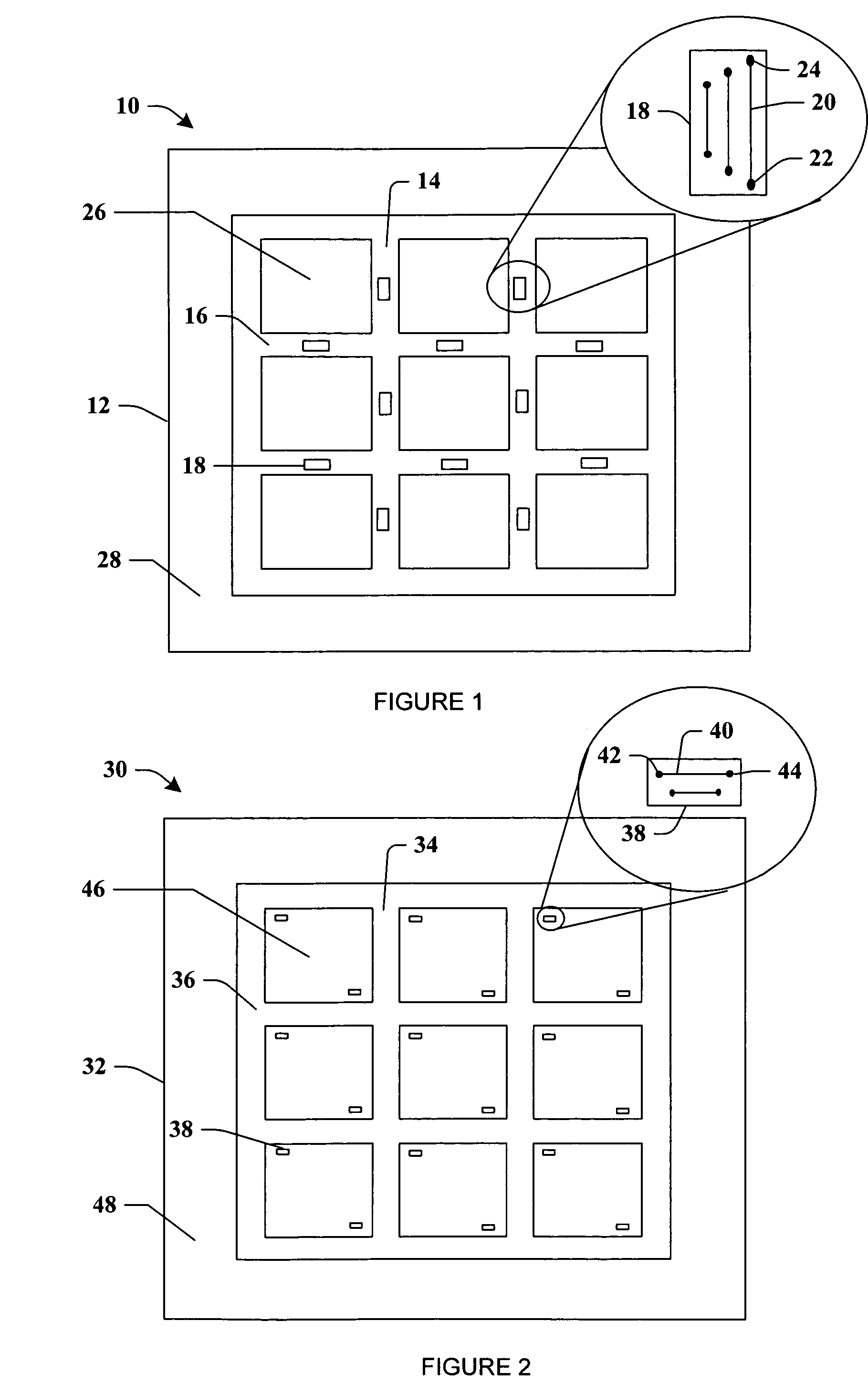
[0033]FIG. 1 illustrates reticle 10 in accordance with one aspect of the present invention. In semiconductor integrated circuit fabrication, a reticle is used during the photolithography process to expose a resist layer coated on a wafer corresponding to the pattern formed on the reticle. The reticle 10 includes a plurality of device feature areas 26 which are used to expose a plurality of individual die or chips on a wafer or substrate. The device feature area is the area of the reticle where the features of the integrated circuits are located. Each device feature ...


PUM


Abstract

A system for testing a reticle used in semiconductor wafer fabrication is provided. The system includes a reticle that has an opaque metal layer over a translucent substrate. The reticle includes one or more test features containing probe points operable for electrical contact. The system includes a reticle test system that is capable of applying a voltage to the probe points, measuring the resulting current, calculating the corresponding resistance of the test features, and determining the critical dimensions of the test features. The system is also capable of determining defects based on the resistance measurements. The critical dimension information and defect information can then be used to refine the processes used in the fabrication of subsequent reticles.

Description

FIELD OF THE INVENTION[0001]The present invention generally relates to semiconductor processing and, more particularly, to a system and method for facilitating the development of a reticle employed in semiconductor processing.BACKGROUND OF THE INVENTION[0002]In the semiconductor industry, there is a continuing trend toward higher device densities. To achieve these high densities there have been, and continue to be, efforts toward scaling down device dimensions (e.g., at sub-micron levels) on semiconductor wafers. In order to accomplish such high device packing densities, smaller and smaller feature sizes are required. This may include the width and spacing of interconnecting lines, spacing and diameter of contact holes, and the surface geometry, such as corners and edges, of various features. The dimensions of and between such small features can be referred to as critical dimensions.[0003]The requirement of small features with close spacing between adjacent features requires high re...

Claims


Application Information

Patent Timeline
IPC IPC(8): G01R27/08G03F1/00G03F1/14H01L23/544
CPCG03F1/14G03F1/44G03F1/84H01L22/34
Inventor LYONS, CHRISTOPHER F.PHAN, KHOI A.TABERY, CYRUS E.SINGH, BHANWAR
Owner GLOBALFOUNDRIES INC
Why Eureka
Try Eureka