Method to measure oxide thickness by FTIR to improve an in-line CMP endpoint determination

a silicon oxide and endpoint measurement technology, applied in the field of metalrology methods for measuring film thickness, can solve the problems of affecting the quality of several, excessive surface non-planarity, and more severe constraints on the degree of planarity,

Inactive Publication Date: 2005-05-17
TAIWAN SEMICON MFG CO LTD
View PDF13 Cites 19 Cited by
  • Summary
  • Abstract
  • Description
  • Claims
  • Application Information

AI Technical Summary

Problems solved by technology

As device sizes decrease, the importance of achieving high resolution features through photolithographic processes correspondingly increases thereby placing more severe constraints on the degree of planarity required of a semiconductor wafer processing surface.
Excessive degrees of surface non-planarity will undesirably affect the quality of several semiconductor manufacturing process including, for example, photolithographic patterning processes, where the positioning the image plane of the process surface within an increasingly limited depth of focus window is required to achieve high resolution semiconductor feature patterns.
Further, over polishing may result in scratching of surface features where over polishing of the underlying layer is formed of a harder material.
Since slurries are frequently insufficiently selective to prevent such over polishing, CMP processes typically employ an endpoint detection system to determine a point at which the underlying layer is exposed.
In-situ optical de

Method used


Image

  • Method to measure oxide thickness by FTIR to improve an in-line CMP endpoint determination
  • Method to measure oxide thickness by FTIR to improve an in-line CMP endpoint determination
  • Method to measure oxide thickness by FTIR to improve an in-line CMP endpoint determination

Examples


Embodiment Construction

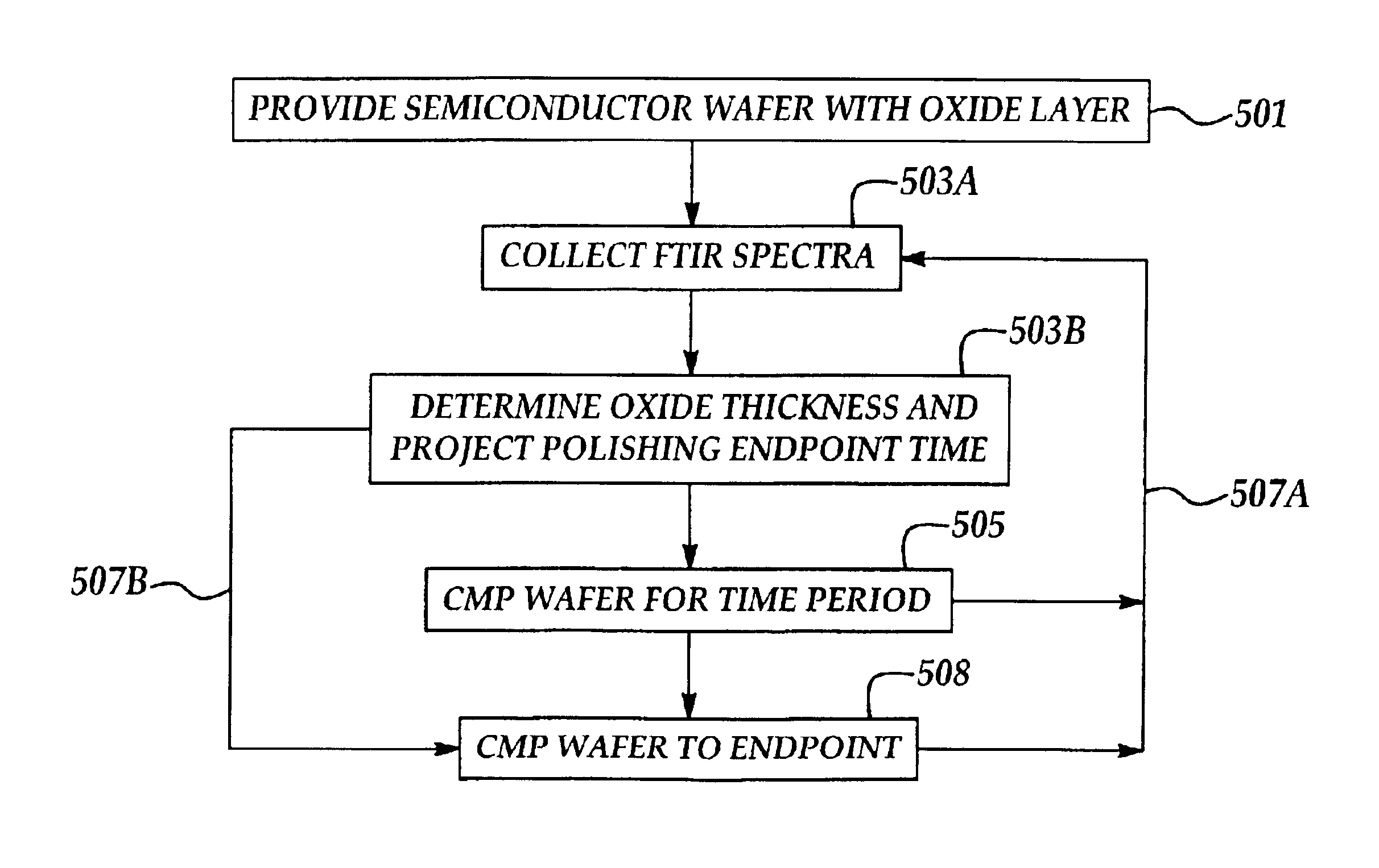
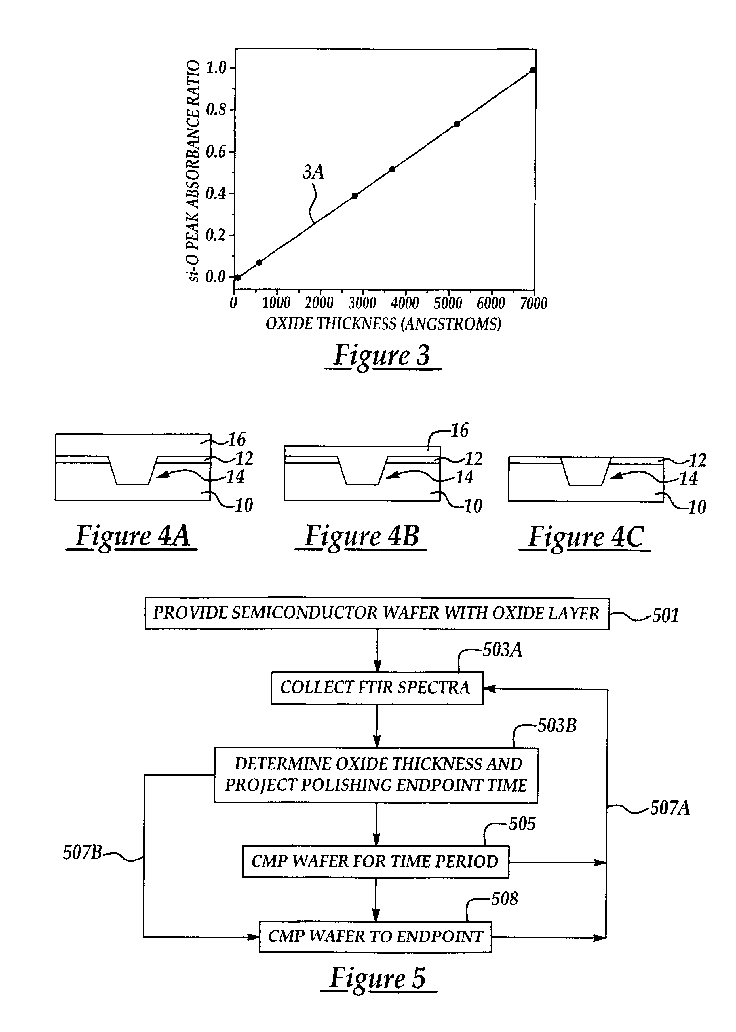
[0017]Although the method of the present invention is explained in exemplary implementation for use in a semiconductor wafer CMP process to monitor a thickness or presence of an oxide layer undergoing a CMP process, it will be appreciated that the method of the present invention may be advantageously used to quickly and easily measure the remaining thickness or presence of an oxide layer in any semiconductor manufacturing process.

[0018]In a first embodiment of the present invention a semiconductor wafer process surface having an exposed surface portion is provided. An infrared (IR) source of energy (probe) is directed at the process surface and at least one Fourier Transform Infrared (FT-IR) spectra including a detected signal intensity is collected from at targeted measurement area of the process surface including a predetermined bandwidth of frequencies characteristic of at least one vibrational frequency mode characteristic of material present in the pathway of the IR probe. The ...


PUM


Abstract

A method for determining a material layer thickness transmissive to infrared (IR) energy in a semiconductor wafer manufacturing process including providing at least one semiconductor wafer comprising an IR transmissive layer; passing IR energy through the IR transmissive layer to produce at least one Fourier transform infrared (FTIR) spectrum; and, determining an amount of the IR transmissive layer present according to an amount of IR energy absorbed by a predetermined contributing characteristic vibrational mode portion of the FTIR spectrum.

Description

FIELD OF THE INVENTION[0001]This invention generally relates to metrology methods for measuring film thicknesses and more particularly to a method for measuring a silicon oxide film thickness in a semiconductor wafer microelectronic manufacturing process, for example for use as an in-line metrology tool for endpoint determination in a chemical mechanical polishing CMP process.BACKGROUND OF THE INVENTION[0002]Planarization is increasingly important in semiconductor manufacturing techniques. As device sizes decrease, the importance of achieving high resolution features through photolithographic processes correspondingly increases thereby placing more severe constraints on the degree of planarity required of a semiconductor wafer processing surface. Excessive degrees of surface non-planarity will undesirably affect the quality of several semiconductor manufacturing process including, for example, photolithographic patterning processes, where the positioning the image plane of the proce...

Claims


Application Information

Patent Timeline
IPC IPC(8): G01B11/06B24B37/04B24B49/12
CPCB24B37/042G01B11/0625B24B49/12
Inventor LIU, AI-SENJANG, SYUN-MING
Owner TAIWAN SEMICON MFG CO LTD
Why Eureka
Try Eureka