Production method for semiconductor wafer

a production method and technology for semiconductors, applied in the direction of flexible wheel, manufacturing tools, lapping machines, etc., can solve the problems of increased operator work load and apparatus size, increased industrial waste (waste lapping powder) due to the increase in used materials, increased size, etc., to achieve excellent finished surface, reduce cost, and reduce grinding damage

Inactive Publication Date: 2007-02-01
SUMCO CORP
View PDF8 Cites 20 Cited by
  • Summary
  • Abstract
  • Description
  • Claims
  • Application Information

AI Technical Summary

Benefits of technology

[0009] Therefore, according to the method of the invention, an excellent finished surface with relatively less grinding damage can be obtained very efficiently, and minute surface undulations generated by the slicing process or the double disc grinding process can be removed. Furthermore, the concentration of the abrasive grains in the slurry is lowered to about one-tenth of the usual concentration. Thus, the amount of the abrasive grains used is small, and cost reduction can be achieved by the reduct...

Problems solved by technology

However, a lapping apparatus for use in the lapping processes in the conventional production methods for a semiconductor wafer described above is increased in size with wafer size enlargement, and pressing problems arise such as increases in consumable materials cost and apparatus cost, operators' work load and apparatus size with increased wafer size, and an increase in industrial wastes (waste lapping powder) due to the increase in used materials.
Furthermore, when single side grinding is conducted right after slicing, there is a problem that undulations generated by ...

Method used


Image

  • Production method for semiconductor wafer
  • Production method for semiconductor wafer
  • Production method for semiconductor wafer

Examples


example

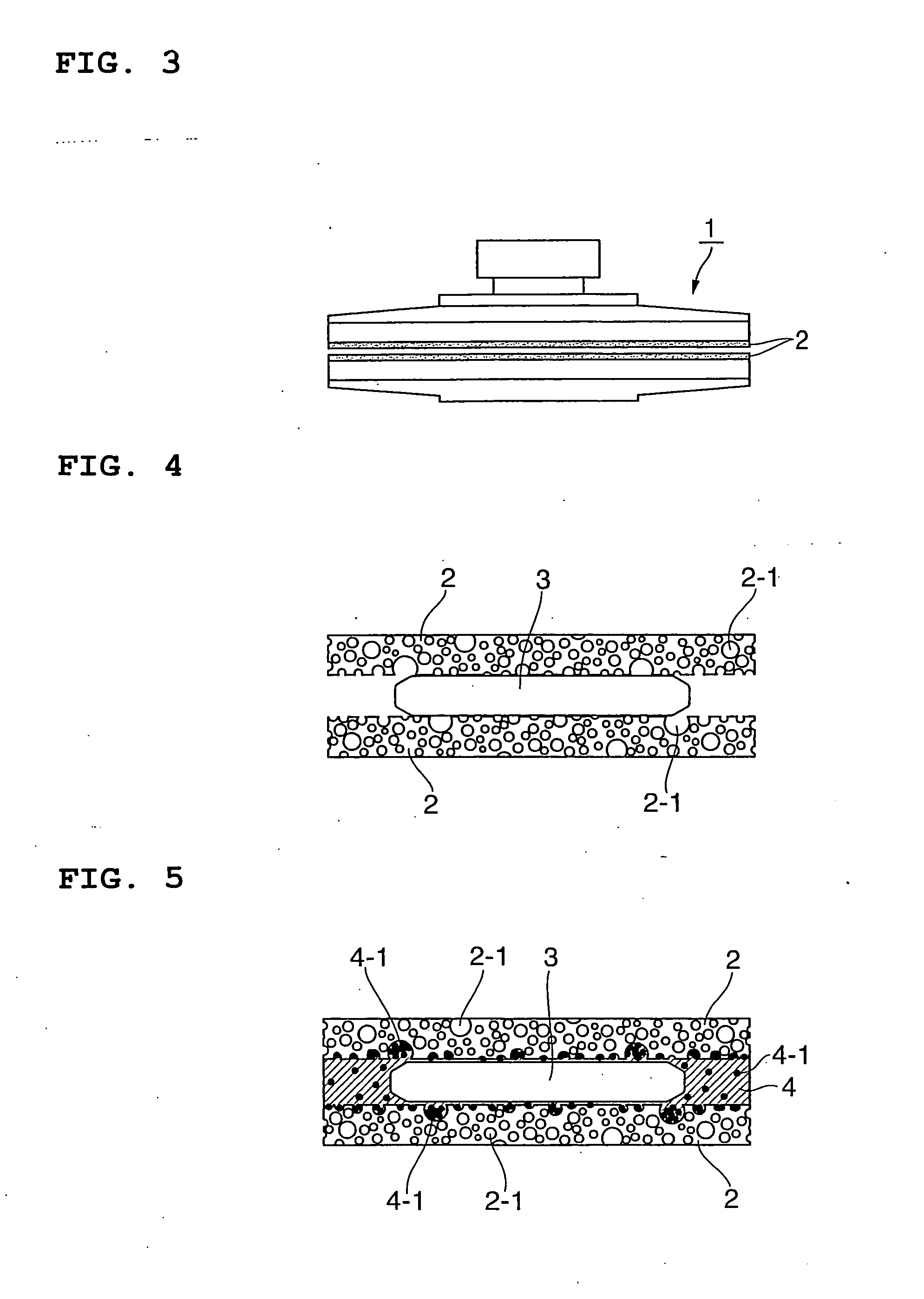
[0024] A slurry of GC #800 abrasive grains having a concentration of 0.3 wt % was supplied to a double side polisher (FIG. 3) having a porous closed-cell polyurethane pad attached, and semi-fixed abrasive grinding was conducted. Consequently, in a 300 mm wafer, a semi-mirror surface semiconductor wafer was obtained with stock removal rate=2 to 5 μm / min, flatness TTV <1.0 μm, and the surface roughness Ra <400 angstrom.

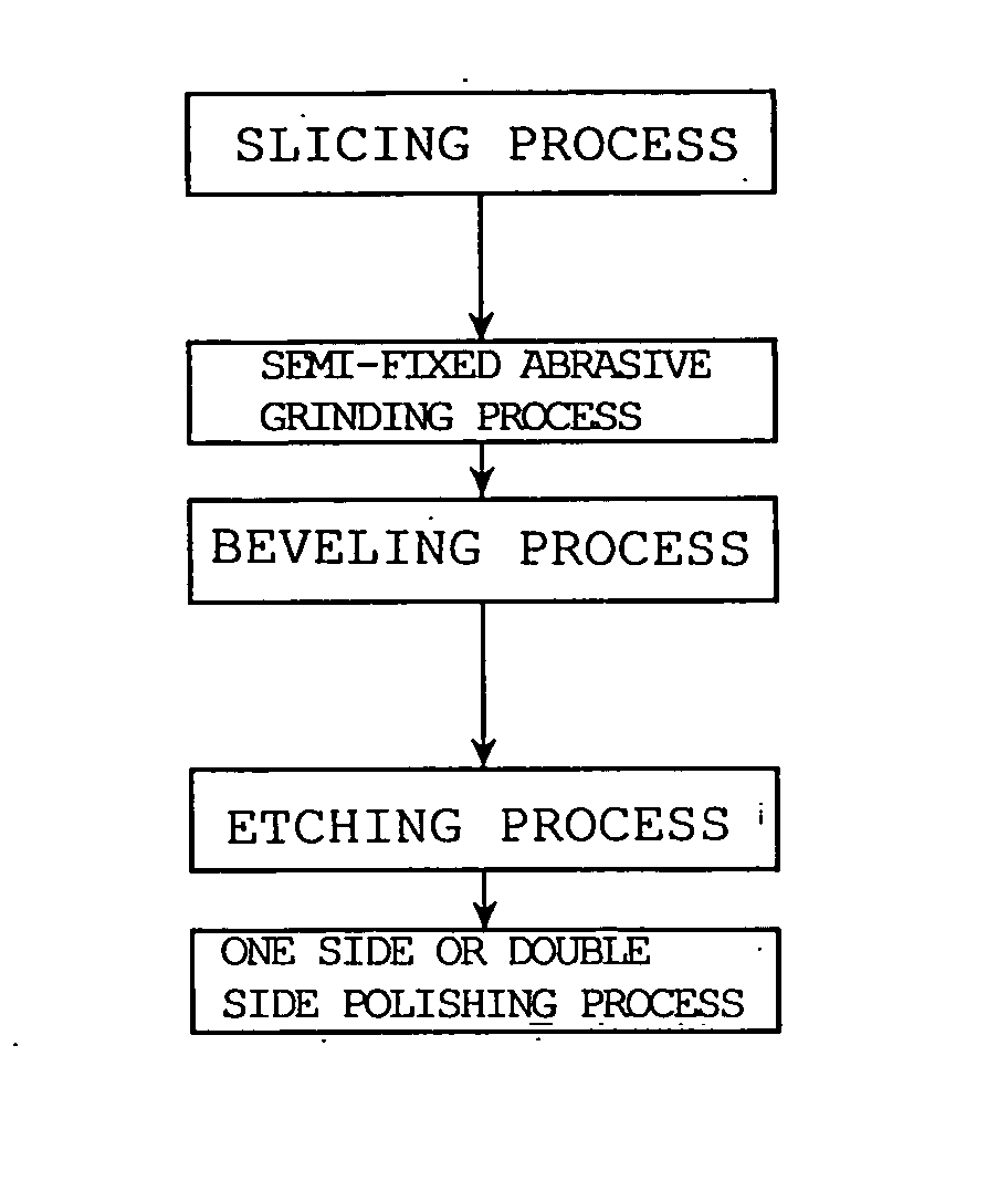
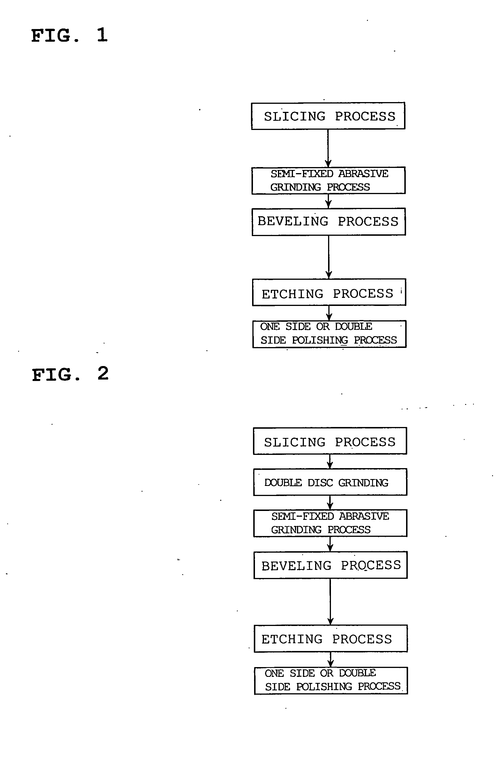
[0025] Furthermore, the process method (semi-fixed abrasive grinding) was incorporated appropriately in the fabrication process steps shown in FIGS. 1 and 2 to fabricate semiconductor wafers. The results of reductions in thickness of the removed portion and minute surface undulations (nanotopography) compared to the conventional fabrication process shown in FIG. 7 are shown in Table 1.

[0026] As apparent from the results in Table 1, with respect to a nanotopography value of 24.9 nm in the 10 mm square size in the conventional process (FIG. 7), it was 24.7 nm in the fab...


PUM

PropertyMeasurementUnit
Abrasiveaaaaaaaaaa
Semiconductor propertiesaaaaaaaaaa

Abstract

A production method for a semiconductor wafer is provided in which semi-fixed abrasive grain grinding with free abrasive grains reduces minute surface undulations generated by wire saw slicing or double disc grinding as well as simplifying conventional semiconductor wafer fabrication process steps. A production method for a semiconductor wafer characterized by conducting a slicing process, then a beveling process, an etching process, and a one side or double side polishing process, wherein a semi-fixed abrasive grinding process using a porous polishing pad and free abrasive grains is conducted after the slicing process.

Description

TECHNICAL FIELD [0001] The present invention relates to a method of obtaining from a single crystal ingot a semiconductor wafer with high flatness and low deformation under processing, more particularly to a production method for a semiconductor wafer with which semi-fixed abrasive grinding with free abrasive grains reduces minute surface undulations generated by wire saw slicing or double disc grinding while planarizing a semiconductor wafer as well as simplifying conventional semiconductor wafer fabrication process steps. BACKGROUND ART [0002] Generally, a production method for a semiconductor wafer adopts the following process steps: 1) A slicing process which slices a single crystal ingot taken from a single crystal growing apparatus to obtain thin disk-shaped wafers. 2) A beveling process which prevents wafers from chipping and cracking. 3) A lapping process which planarizes beveled wafers. 4) An etching process which removes a grinding damage layer occurred in wafer surfac...

Claims


Application Information

Patent Timeline
IPC IPC(8): C03C15/00H01L21/461B44C1/22B24B7/17B24B9/06B24B37/00B24D13/14H01L21/304H01L21/306
CPCB24B7/17B24B9/065B24B37/042H01L21/30625B24B37/245H01L21/02008H01L21/02013B24B37/08H01L21/304H01L21/30
Inventor ASAKAWA, KEIICHIRO
Owner SUMCO CORP
Why Eureka
Try Eureka