Automatically sharp field emission cathodes

a cathode and automatic technology, applied in the field of electrochemical field emission cold cathodes, can solve the problems of poor uniformity in the curvature radius of the tip, and achieve the effects of smooth surface morphology, improved uniformity, and improved sharpness of the tip

Inactive Publication Date: 2001-03-13
THE UNITED STATES OF AMERICA AS REPRESENTED BY THE SECRETARY OF THE NAVY
View PDF5 Cites 70 Cited by
  • Summary
  • Abstract
  • Description
  • Claims
  • Application Information

AI Technical Summary

Benefits of technology

It is another object of this invention to fabricate a cold cathode field emitter by fabricating the gate before the tips so that sharpness of the tips is not compromised.
It is another object of this invention to fabricate tips by epitaxial techniques which produce tips with far better uniformity and significantly smoother surface morphology than either the oxidation process or deposition of polycrystalline material.

Problems solved by technology

This approach suffers from nonuniform characteristics of the sharp tip due to nonuniform etching and oxidation processes which results in poor uniformity in the tips' radius of curvature.

Method used


Image

  • Automatically sharp field emission cathodes
  • Automatically sharp field emission cathodes
  • Automatically sharp field emission cathodes

Examples


Embodiment Construction

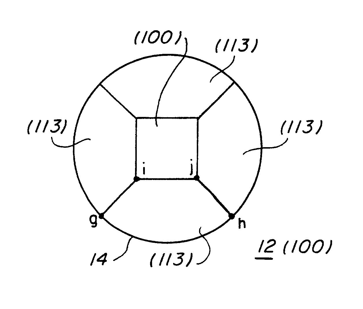
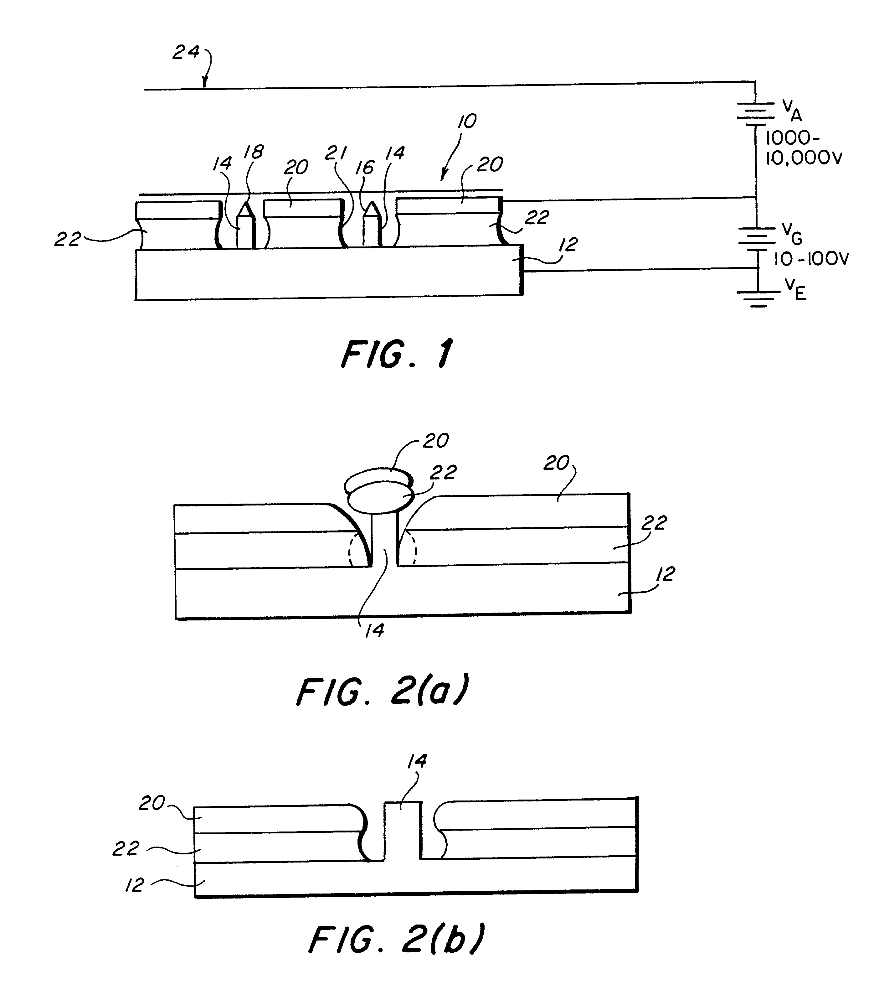
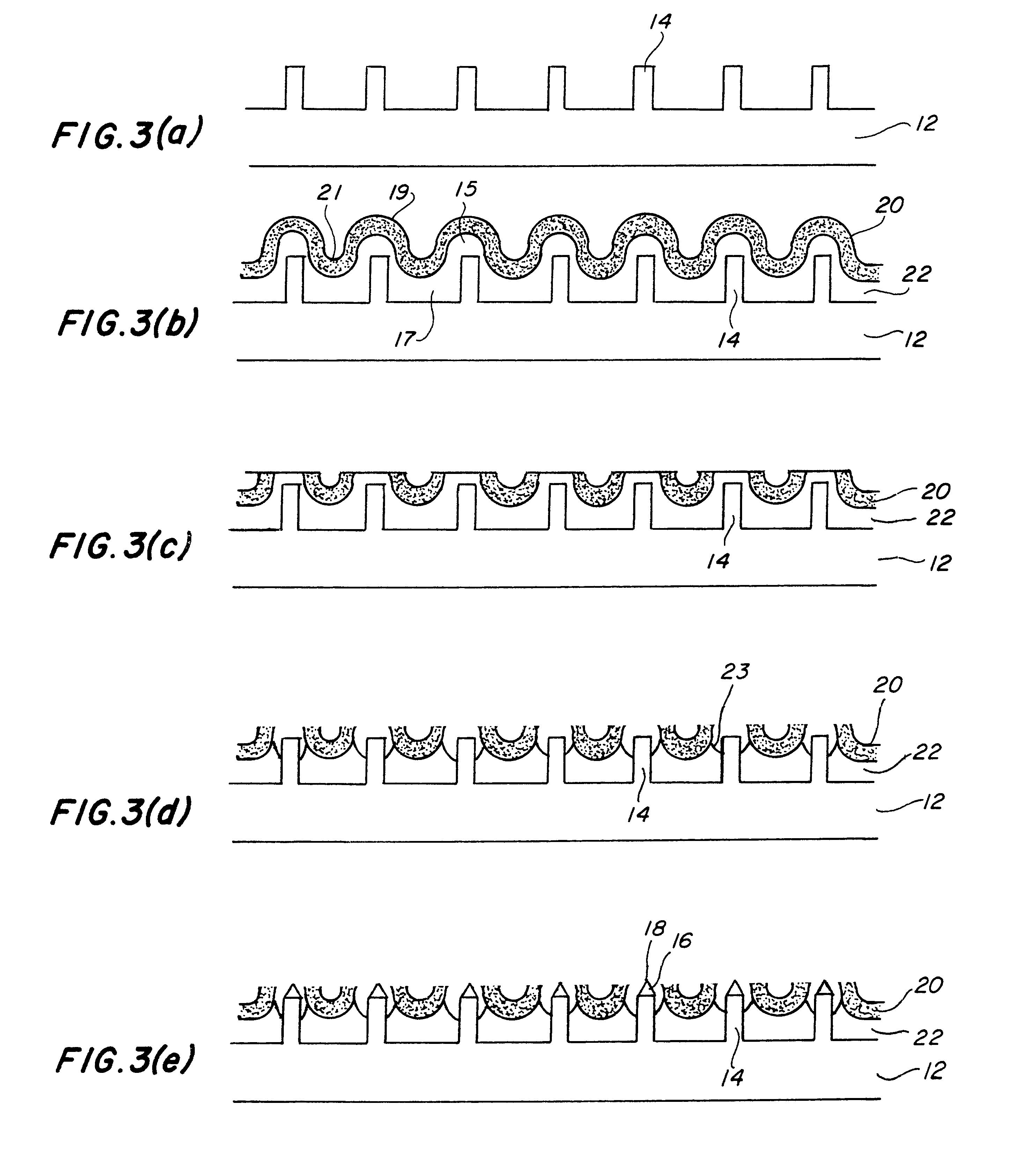
The field emitter array of this invention includes a plurality of semiconducting nanomesas disposed on a semiconducting substrate, microscopic three-dimensional monocrystalline emitting regions or tips on the nanomesas of a semiconducting material each terminating in an apex, and a gate around the nanomesas to provide an extraction bias voltage for field emission such that the emitted electrons travel from the apexes of the tips to the anode when the field emitter is in operation. The gate is supported by a dielectric material disposed on the substrate. The fabrication process generally includes lithography and etching to form nanomesas disposed on a substrate, gate fabrication by directional or conformal deposition and etching, and tip formation by epitaxial self-assembly of semiconducting material deposited on the nanomesas which tips terminate in atomically sharp apexes.

The unique physical property of self-assembly by vapor phase epitaxial growth is used to create atomically shar...


PUM


Abstract

An electron emitting device characterized by a monocrystalline substrate, a plurality of monocrystalline nanomesas or pillars disposed on the substrate in a spaced relationship and extending generally normally therefrom, monocrystalline self-assembled tips disposed on top of the nanomesas, and essentially atomically sharp apexes on the tips for field emitting electrons. A method for making the emitters is characterized by forming a gate electrode and gate electrode apertures before forming the tips on the nanomesas.

Description

BACKGROUND OF INVENTION1. Field of InventionThe present invention relates to the field of electron field emission cold cathodes which have atomically sharp tips and to a fabrication method for making such cathode emitters by fabrication of the gate before the field emitters.2. Description of Prior ArtField emission sources require sharp electron emitter structures to create electric field enhancement which promotes electron emission from the tip of the field emitter. The very sharp structures that are required for field emission cathodes have been primarily fabricated by two approaches. The first approach typically starts with a silicon wafer and uses anisotropic crystallographic etching techniques or isotropic etching techniques in combination with oxidation sharpening to form sharp field emitters. A gate structure for modulating the emission current is fabricated after the tip is created. This approach suffers from nonuniform characteristics of the sharp tip due to nonuniform etch...

Claims


Application Information

Patent Timeline
Patent Type & Authority Patents(United States)
IPC IPC(8): H01J9/02
CPCH01J9/025H01J2201/30426
Inventor HOBART, KARL D.KUB, FRANCIS J.GRAY, HENRY F.TWIGG, MARK E.THOMPSON, PHILLIP E.SHAW, JONATHAN
Owner THE UNITED STATES OF AMERICA AS REPRESENTED BY THE SECRETARY OF THE NAVY
Why Eureka
Try Eureka