Method of forming a gate in a stack gate flash EEPROM cell

a technology of stack gate and flash eeprom cell, which is applied in the direction of semiconductor devices, electrical apparatus, transistors, etc., can solve the problems of deteriorating the operation speed of the entire cell and erase the effect of the ga

Inactive Publication Date: 2001-03-20
HYUNDAI ELECTRONICS IND CO LTD
View PDF12 Cites 27 Cited by
  • Summary
  • Abstract
  • Description
  • Claims
  • Application Information

AI Technical Summary

Problems solved by technology

Consequently, it causes a deteriorati...

Method used


Image

  • Method of forming a gate in a stack gate flash EEPROM cell
  • Method of forming a gate in a stack gate flash EEPROM cell

Examples


Embodiment Construction

Hereinafter, the preferred embodiments in accordance with the present invention will be described in detail with reference to the accompanying drawings.

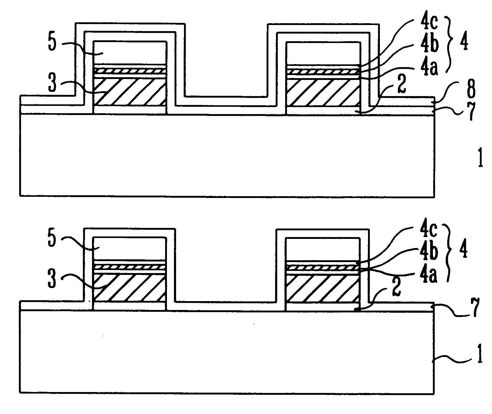
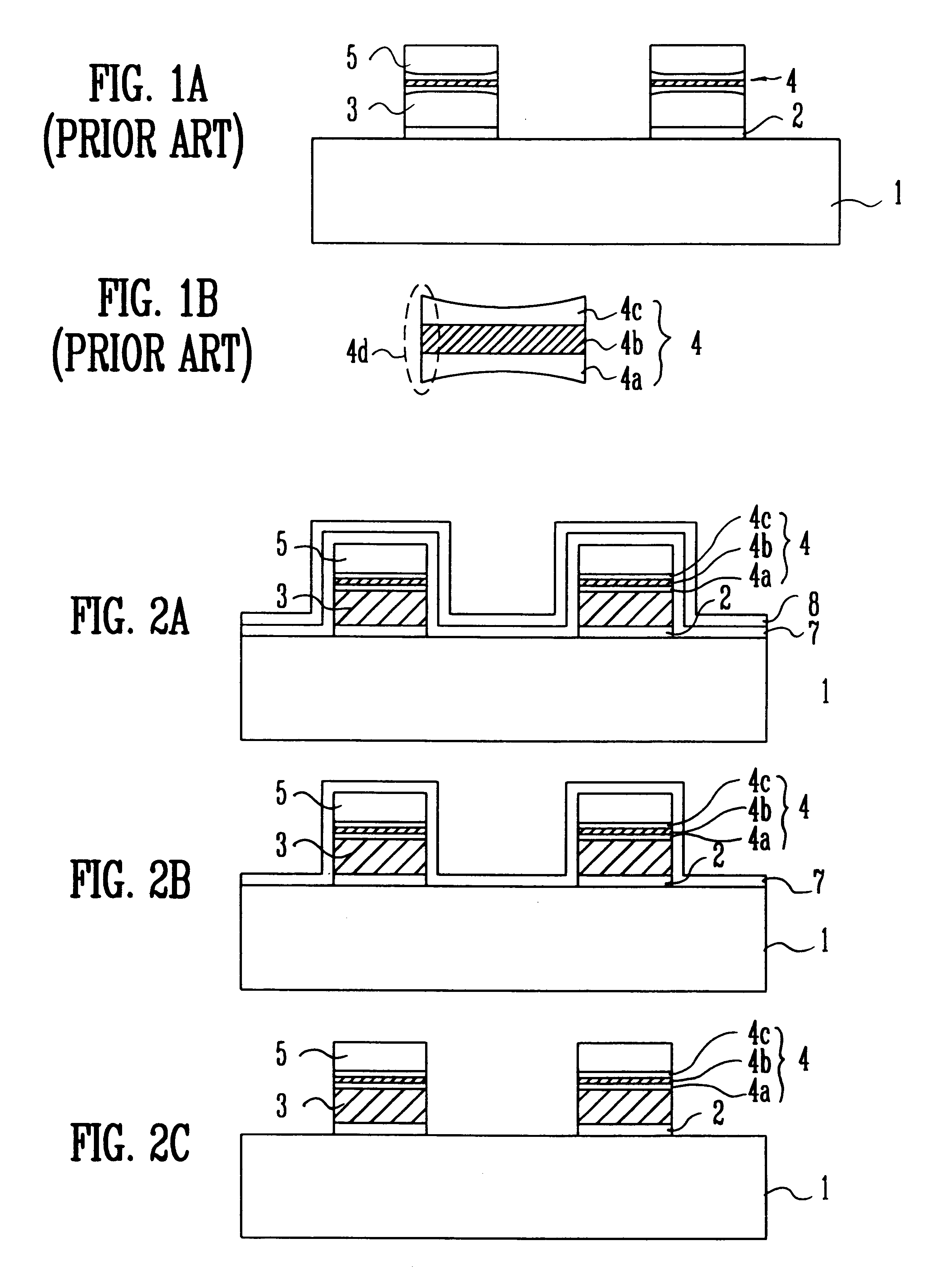
FIGS. 2A to 2C are cross-sectional views showing a method of forming a gate in a stack gate flash EEPROM cell in accordance with the present invention.

FIG. 2A is a cross-sectional view illustrating a stack gate formed by stacking a floating gate 3 and a control gate 5 on a semiconductor substrate 1. A tunnel oxide layer 2 is formed between the floating gate 3 and the semiconductor substrate 1. A dielectric layer 4 is formed between the floating gate 3 and the control gate 5. The dielectric layer 4 is an ONO structure formed by stacking a lower oxide layer 4a, a nitride layer 4b and an upper oxide layer 4c. Next, an oxide layer 7 as a first barrier layer is deposited on an entire upper portion including the cell gate to a thickness of 50 to 100 .ANG. under a low temperature of below 775.degree. C. Then, a nitride layer 8 as a second b...


PUM


Abstract

The present invention relates to a method of forming a gate in a stack gate flash EEPROM cell. In order to preventing a lateral bird's beak from occurring in an ONO dielectric layer during a reoxidation process to be performed after a formation of a cell gate having a stack structure formed by stacking a floating gate, an ONO dielectric layer and a control gate, an oxide layer and a nitride layer are sequentially formed on an entire structure before the reoxidation and after a formation of the cell gate. The oxide layer serves to reduce a stress in depositing the nitride layer, and the nitride layer serves to prevent an occurrence of the lateral bird's beak of the ONO dielectric layer during the reoxidation process. Accordingly, the present invention prevents the lateral bird's beak of the ONO dielectric layer, thereby improving a speed of cell erase operation.

Description

1. Field of the InventionThe present invention relates to a method of forming a gate in a stack gate flash EEPROM cell and more particularly, to a method of forming a gate in a stack gate flash EEPROM cell capable of improving an erase operation speed by reducing a lateral bird's beak of an ONO dielectric layer and increasing a coupling ratio, wherein the lateral bird's beak occurs during a reoxidation process to be performed after a formation of a cell gate having a stack structure formed by stacking a floating gate, an ONO dielectric layer and a control gate.2. Description of the Prior ArtHereinafter, a method of forming a gate in a conventional stack gate flash EEPROM cell will be described with reference to FIG. 1.In FIG. 1A, there is shown a method of forming a gate in a stack gate flash EEPROM cell. Referring to FIG. 1A, a stack gate having a stack structure of a floating gate 3 and a control gate 5 is formed on a semiconductor substrate 1. A tunnel oxide layer 2 is formed bet...

Claims


Application Information

Patent Timeline
IPC IPC(8): H01L21/02H01L21/28H01L21/70H01L21/8247H01L27/115H01L29/788H01L29/792
CPCH01L21/28273H01L27/11521H01L29/40114H10B41/30H10B69/00
Inventor LEE, KEUN WOOKIM, KI SEOGSHIN, JINPARK, SUNG KEE
Owner HYUNDAI ELECTRONICS IND CO LTD
Why Eureka
Try Eureka