

Photolithographic method
a photolithographic and photoresist technology, applied in the field of integrated circuit manufacturing, can solve the problems of difficult to reproduce the layout of the photomask onto the photoresist in a consistent manner, the resolution is one of the limiting characteristics of the exposure tool, and the layout design is typically quite complicated
- Summary
- Abstract
- Description
- Claims
- Application Information
AI Technical Summary
Problems solved by technology
Method used
Image

Examples
Embodiment Construction
The methods described below involve the use of multiple exposures along with changing the exposure parameters of the photolithographic imaging tool to reduce the proximity effect. It should be noted that these methods may be applicable to many forms of photolithography, including, for example, laser based deep UV, non-laser based deep UV, and x-ray photolithography.
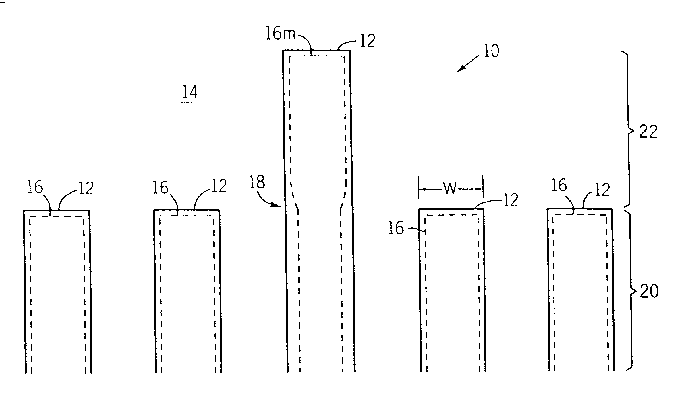
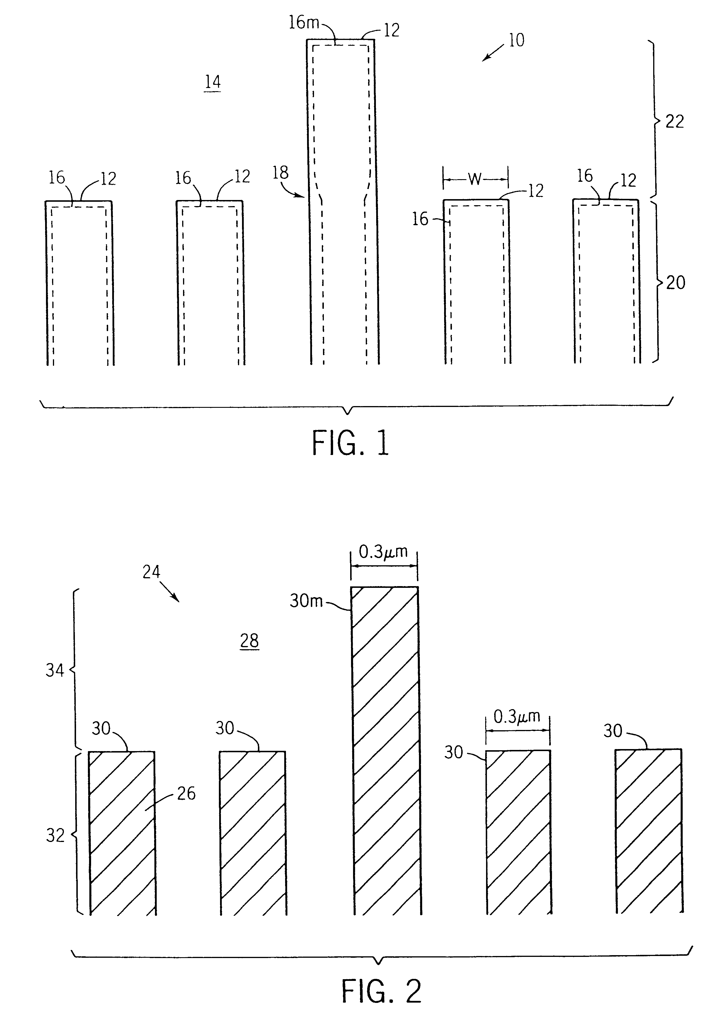
Turning now to the drawings, and referring initially to FIG. 1, a portion 10 of a photomask is shown. The portion 10 of the photomask illustrates five lines 12 defined by opaque regions of the photomask. By irradiating a photoresist-cover substrate 14 which underlies the portion 10 of the photomask with appropriate radiation, five lines 16 may be patterned, i.e., transferred, onto the photoresist-cover substrate 14. It is typically desirable that all five lines 16 be patterned with a width substantially equal to the width W of the lines 12 on the photomask. However, because of the proximity effect, the width of middle lin...
PUM
| Property | Measurement | Unit |
|---|---|---|
| width | aaaaa | aaaaa |
| width | aaaaa | aaaaa |
| width | aaaaa | aaaaa |
Abstract
Description
Claims
Application Information