Silicon-on-insulator wafer having conductive layer for detection with electrical sensors

a technology of silicon-on-insulator wafers and electrical sensors, which is applied in the direction of individual semiconductor device testing, semiconductor/solid-state device testing/measurement, instruments, etc., can solve the problem of incompatibility of tools for manufacturing integrated circuits

Inactive Publication Date: 2001-05-29
IBM CORP
View PDF12 Cites 14 Cited by
  • Summary
  • Abstract
  • Description
  • Claims
  • Application Information

AI Technical Summary

Problems solved by technology

This sensor evolution has rendered these tools incompatible for manufacturing integrated circuits using wafers with properties different than those of silicon wafers.
However, sinc

Method used


Image

  • Silicon-on-insulator wafer having conductive layer for detection with electrical sensors
  • Silicon-on-insulator wafer having conductive layer for detection with electrical sensors
  • Silicon-on-insulator wafer having conductive layer for detection with electrical sensors

Examples


Embodiment Construction

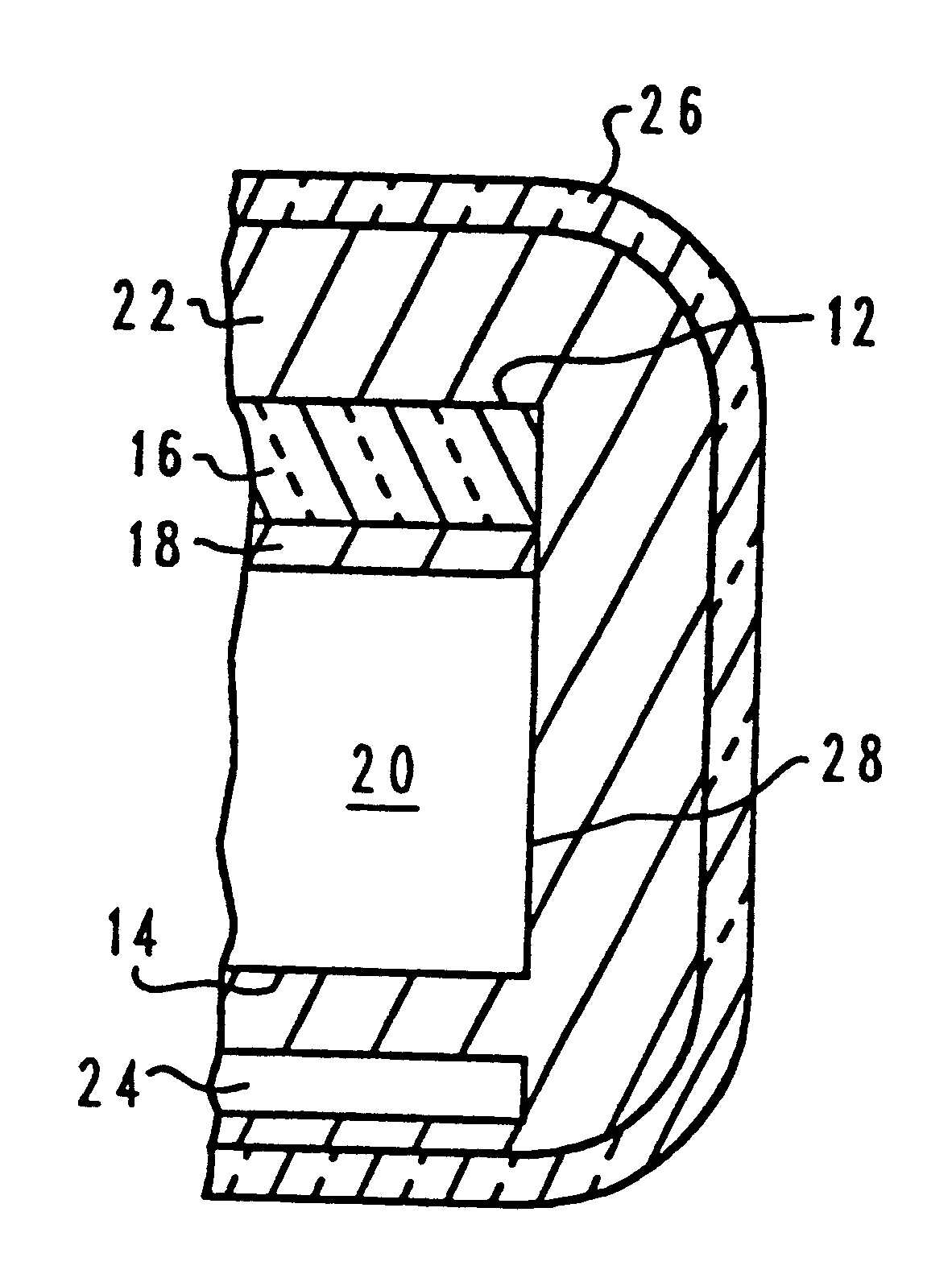
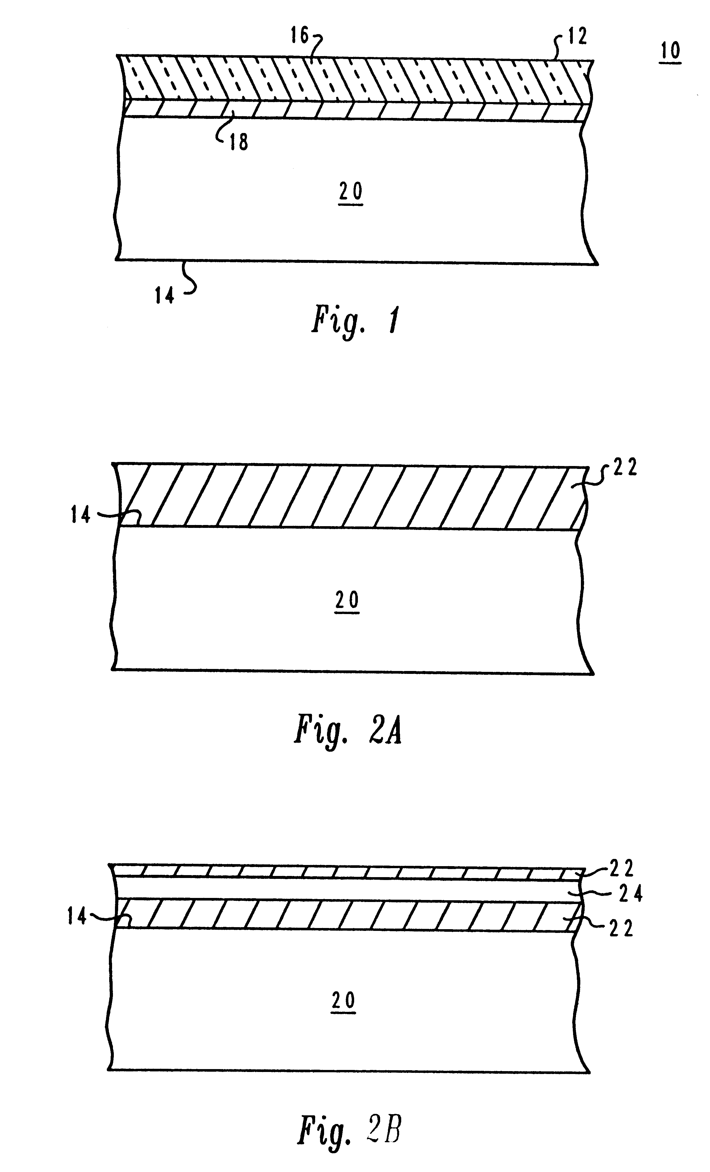
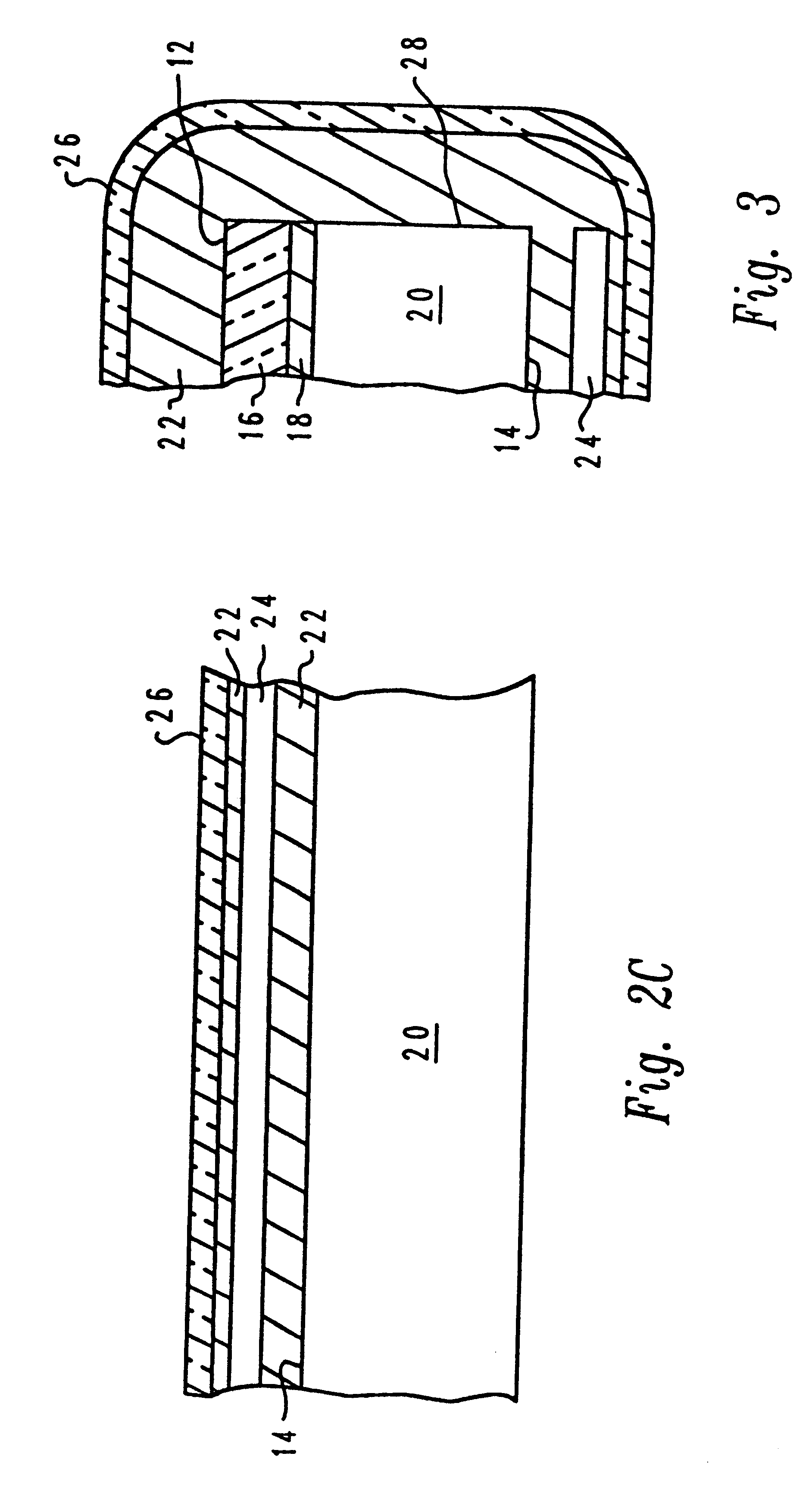
The process steps and structures described below do not form a complete process flow for manufacturing integrated circuits. The present invention can be practices in conjunction with integrated circuit fabrication techniques currently used in the art, and only so much of the commonly practiced process steps are included as are necessary for an understanding of the present invention. The figures representing fragmentary sections of portions of an integrated circuit during fabrication are not drawn to scale, but instead are drawn so as to illustrate the important features of the invention.

The present invention provides a way to process both silicon and SOS wafers on a common production tool set without changing or bypassing robotic wafer sensors. In accordance with a preferred embodiment of the present invention, the SOS wafers are coated with a material that is sufficiently opaque, conductive and compatible with the harsh conditions of a semiconductor manufacturing process to make th...


PUM


Abstract

A method for fabricating a silicon-on-sapphire wafer for processing by silicon-wafer-processing equipment. A layer is deposited on a backside of a silicon-on-sapphire wafer, the layer having optical and electrical properties of silicon, wherein the silicon-on-sapphire wafer may be sensed by a sensor designed to sense a presence of a silicon wafer.

Description

1. Technical FieldThe present invention relates in general to integrated circuits and in particular to a method for manufacturing wafers for use in manufacturing integrated circuits. Still more particularly, the present invention relates to a method for manufacturing a silicon-on-sapphire wafer.2. Description of the Related ArtThe use of sapphire substrates in the production of semiconductor devices, such as silicon-on-sapphire (SOS) devices, has greatly increased. SOS integrated circuit technology is a promising field for advanced high speed integrated circuits for computer and microwave applications.Integrated circuit manufacturing equipment has evolved in recent years through the use of robotic wafer transfer systems. For those robotic wafer transfer systems to function, the robot must be able to sense either optically or electrically the presence of a silicon wafer. These robot sensors have evolved around the properties of a silicon wafer--the sensors are looking for an opaque, ...

Claims


Application Information

Patent Timeline
IPC IPC(8): H01L21/205H01L21/67H01L21/02H01L27/12
CPCH01L21/67H01L21/02658H01L21/02664H01L21/0242H01L21/02532H01L21/20
Inventor EGLEY, JAMES L.GUT, GEORGE M.KOCH, DANIEL J.MATUSEWIC, MICHAEL A.
Owner IBM CORP
Why Eureka
Try Eureka