SOS substrate with reduced stress
一种基板、蓝宝石基板的技术,应用在电气元件、晶体管、电固体器件等方向,能够解决电子迁移率下降等问题
- Summary
- Abstract
- Description
- Claims
- Application Information
AI Technical Summary
Problems solved by technology
Method used
Image

Examples
Embodiment 1
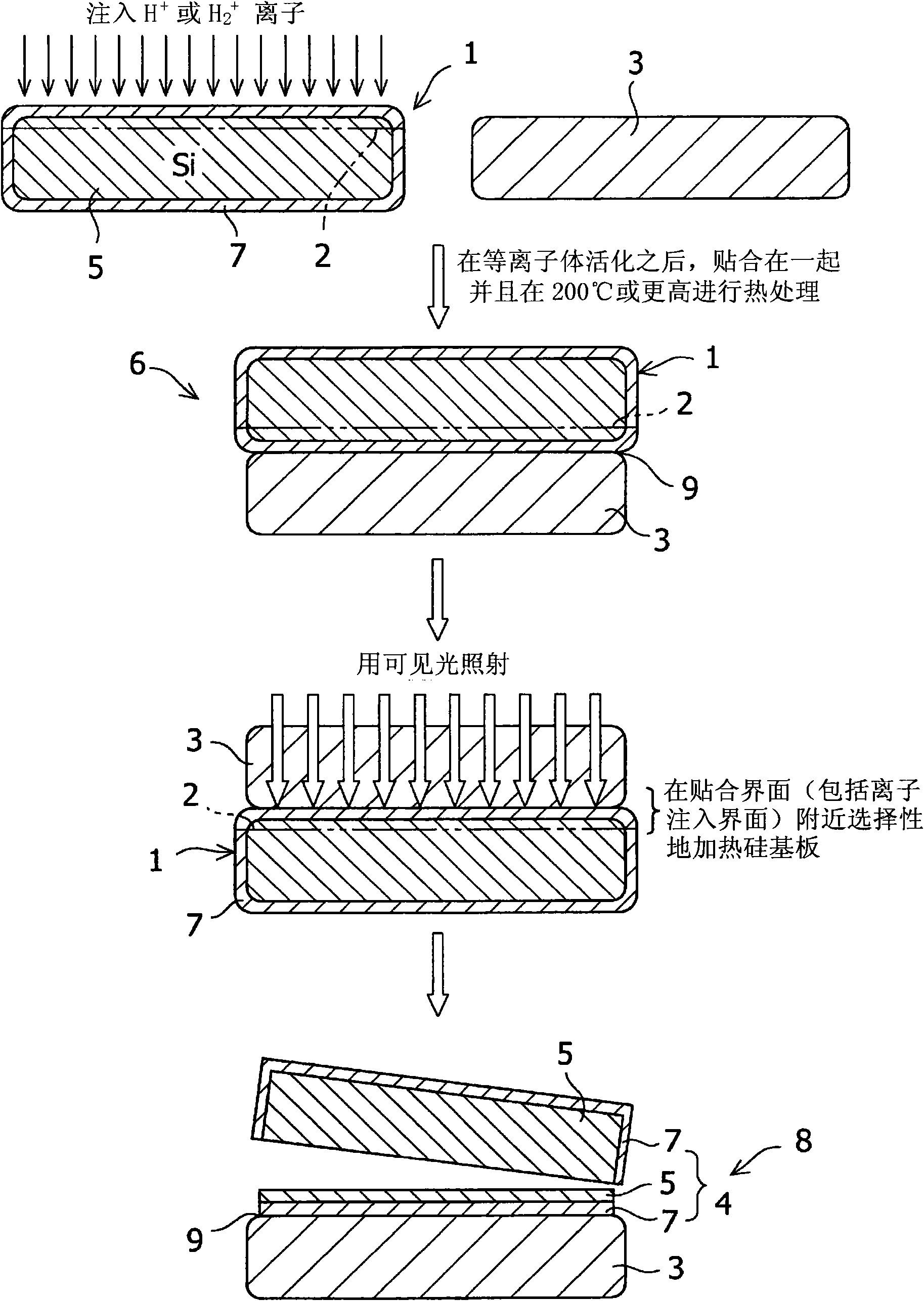
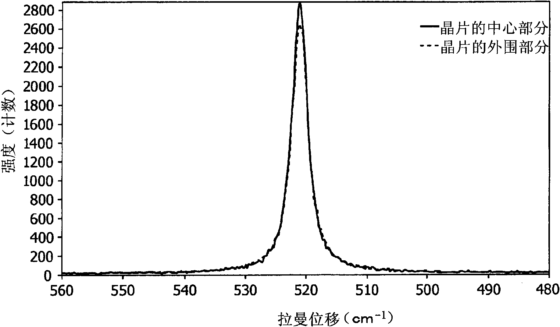
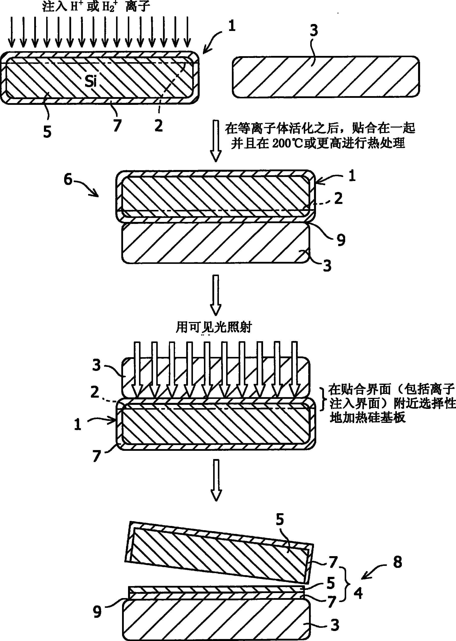
[0083] First grow a 200nm thick oxide film on a silicon substrate (thickness 625μm, diameter 150mm). at 55KeV and 7.0×10 16 atom / cm 2 A dose of hydrogen ions (H + ). The surfaces of both the sapphire substrate and the silicon substrate were subjected to ion beam activation treatment and bonded together at 200°C. The two substrates were heat-treated at 225° C. for 24 hours and temporarily bonded together, and then cooled to room temperature. Subsequently, the bonded substrates were placed on a hot plate at 200° C., and a mechanical impact was applied to the bonded interface to cause peeling, thereby transferring the silicon film to the sapphire substrate. This confirmed the transfer of the silicon film to the entire surface of the sapphire substrate. The silicon layer of the substrate was polished by CMP to have a thickness of 200 nm. figure 2 The results of Raman shift measurement of this silicon film are shown. The Raman shift of the central part is 520.94cm -1 , the...
Embodiment 2
[0085] First grow a 200nm thick oxide film on a silicon substrate (thickness 625μm, diameter 150mm). at 55KeV and 7.0×10 16 atom / cm 2 A dose of hydrogen ions (H + ). The surfaces of both the sapphire substrate and the silicon substrate were subjected to plasma activation treatment and bonded together at 350°C. The two substrates were heat-treated at 225° C. for 24 hours and temporarily bonded together, and then cooled to room temperature. Subsequently, the bonded substrates were heated to 300° C. on a hot plate, and a mechanical impact was applied to the bonded interface to cause peeling, thereby transferring the silicon film to the sapphire substrate. This confirmed the transfer of the silicon film to the entire surface of the sapphire substrate. The silicon layer of the substrate was polished by CMP to have a thickness of 200 nm. The Raman shift of the central part is 521.28cm -1 , the Raman shift of the peripheral part is 521.10cm -1 . The Raman shift of bulk silic...
Embodiment 3
[0087] First grow a 200nm thick oxide film on a silicon substrate (thickness 625μm, diameter 150mm). at 55KeV and 7.0×10 16 atom / cm 2 A dose of hydrogen ions (H + ). The surfaces of both the sapphire substrate and the silicon substrate were subjected to plasma activation treatment and bonded together at 200°C. The two substrates were heat-treated at 225° C. for 24 hours and temporarily bonded together, and then cooled to room temperature. Subsequently, the bonded substrates were heated to 250° C. on a hot plate, and irradiated with YAG laser light having a wavelength of 523 nm. A mechanical shock is applied to the bonded interface to cause debonding, thereby transferring the silicon film to the sapphire substrate. This confirmed the transfer of the silicon film to the entire surface of the sapphire substrate. The silicon layer of the substrate was polished by CMP to have a thickness of 200 nm. The Raman shift of the central part is 521.25cm -1 , the Raman shift of the ...
PUM
| Property | Measurement | Unit |
|---|---|---|
| compressive stress | aaaaa | aaaaa |
| wavelength | aaaaa | aaaaa |
| diameter | aaaaa | aaaaa |
Abstract
Description
Claims
Application Information