Circuit and Method for Improving ESD Tolerance and Switching Speed

a technology of electrostatic discharge and switching speed, applied in the field of electrostatic discharge tolerance and switching speed improvement, can solve the problems of ic affecting other circuit parameters, damage to a fet, and poor linearity of conventional rf signal switch ic capable of switching at high speed, so as to improve the fet structure having accumulated charge sink (acs) circuit, improve esd tolerance, and fast switching time

Active Publication Date: 2015-05-28
PSEMI CORP
View PDF2 Cites 5 Cited by
  • Summary
  • Abstract
  • Description
  • Claims
  • Application Information

AI Technical Summary

Benefits of technology

[0011]More specifically, embodiments of the invention provide an improved FET structure having accumulated charge sink (ACS) circuit, fast switching times, and improved ESD tolerance. Disclosed embodiments include circuit architectures that include a FET having a gate resistor and an ACS circuit, with the addition of respective (alternative) ACS resistors coupled to the ACS circuit and (directly or indirectly) a node on one side or the other of the corresponding gate resistor (i.e., parallel versus series connected to the gate resistor).
[0012]By inserting larger resistance value ACS resistors in series with the ACS circuit, duri

Problems solved by technology

For example, a conventional RF signal switch IC capable of switching at high speed may exhibit poor linearity, while a highly linear RF signal switch IC may be only capable of switching at much lower frequencies.
Such an ESD event may cause damage to a FET (e.g., gate-oxide punch-through), especially complementary metal-oxide-semi

Method used


Image

  • Circuit and Method for Improving ESD Tolerance and Switching Speed
  • Circuit and Method for Improving ESD Tolerance and Switching Speed
  • Circuit and Method for Improving ESD Tolerance and Switching Speed

Examples


Embodiment Construction

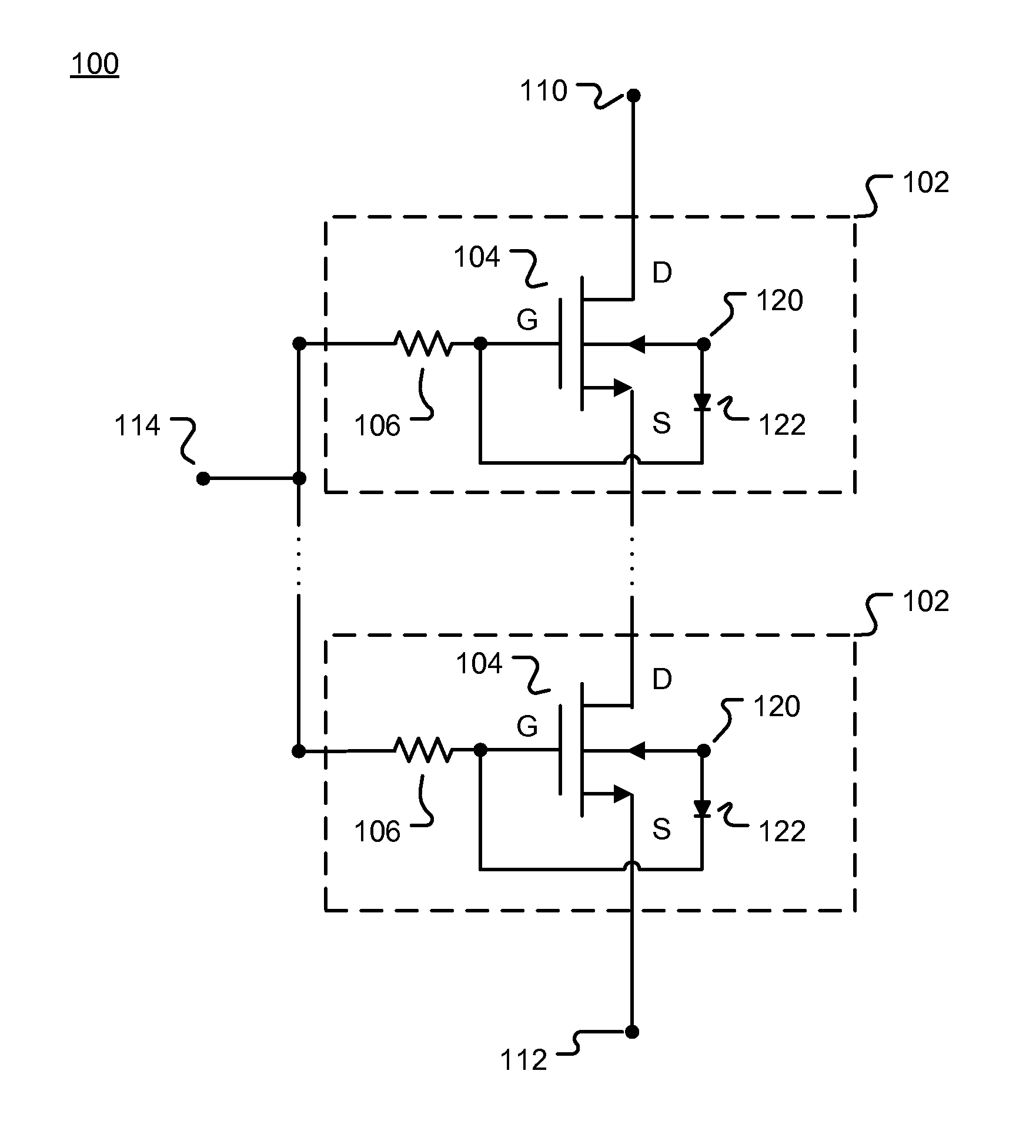
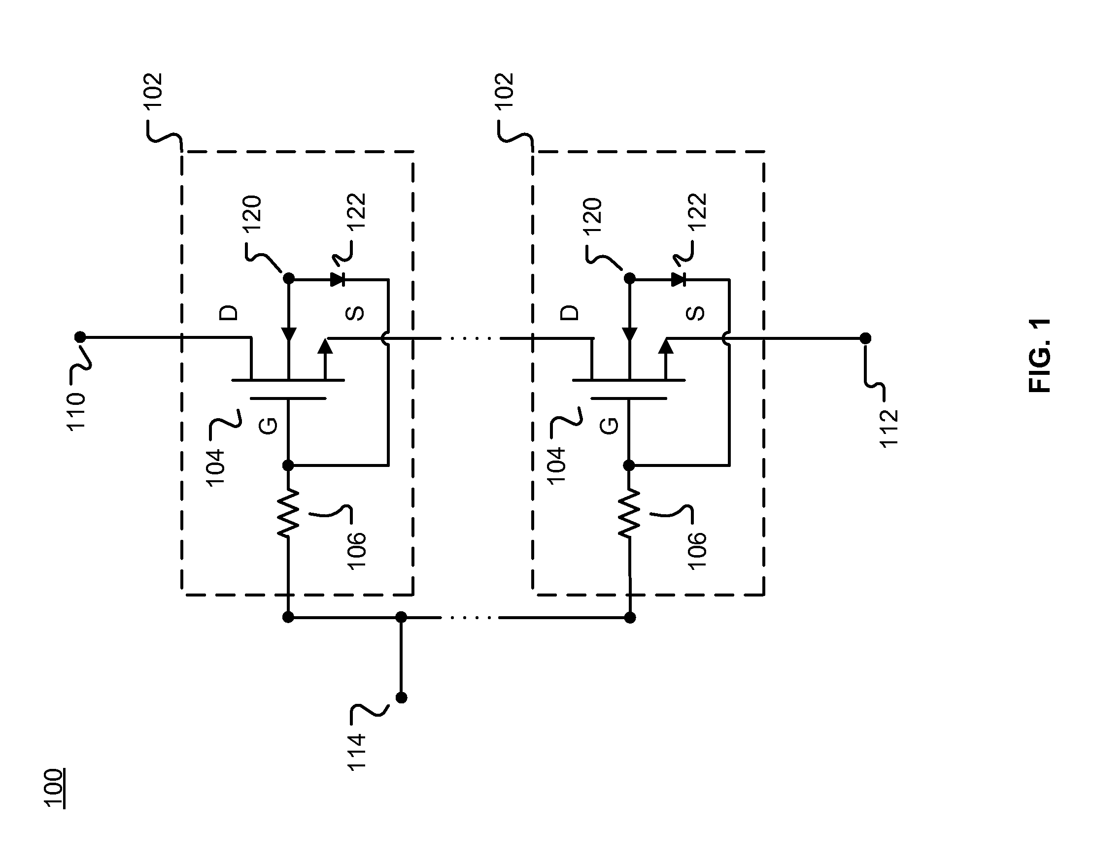
[0018]FIG. 1 is a simplified block diagram of a circuit architecture 100 with stacked semiconductor devices and accumulated charge sink modules according to various embodiments. Shown are a plurality of switching modules 102 in a stacked configuration. In the illustrated embodiment, each switching module 102 includes a FET 104 that includes conventional drain (D), source (S), and gate (G) connections. Connected to the gate of each FET 104 is a gate resistor 106. In general, the stack height N of the circuit architecture 100 (i.e., the number of stacked switching modules 102) is determined by the amount of voltage that the circuit architecture 100 is required to handle. In some embodiments, only one switching module 102 may be needed. As shown in FIG. 1, the circuit architecture 100 also includes a first port 110 coupled to the drain D of a switching module 102, second port 112 coupled to the source of a switching module 102, and a control signal port 114 coupled to each gate resisto...


PUM


Abstract

Embodiments of systems, methods, and apparatus for improving ESD tolerance and switching time for semiconductor devices including metal-oxide-semiconductor (MOS) field effect transistors (FETs), and particularly to MOSFETs fabricated on semiconductor-on-insulator and silicon-on-sapphire substrates. Embodiments provide an improved FET structure having an accumulated charge sink (ACS) circuit, fast switching times, and improved ESD tolerance.

Description

CROSS-REFERENCE TO RELATED APPLICATIONS[0001]This application claims the benefit of priority from:[0002](1) U.S. Provisional Patent Application No. 61 / 906,843, filed Nov. 20, 2013, entitled “Floating Body Contact Circuit Method for Improving ESD Performance and Switching Speed”, the entire disclosure of which is hereby incorporated by reference; and[0003](2) U.S. patent application Ser. No. 14 / 521,331, filed Oct. 22, 2014, entitled “Floating Body Contact Circuit Method for Improving ESD Performance and Switching Speed”, the entire disclosure of which is hereby incorporated by reference, and which claims priority from U.S. Provisional Patent Application No. 61 / 906,843.BACKGROUND[0004](1) Technical Field[0005]This invention relates to electronic circuits, and more particularly to circuits and methods for improving electrostatic discharge (ESD) tolerance and switching speed in integrated circuits (ICs), such as ICs for radio frequency (RF) signal switching or processing.[0006](2) Backg...

Claims


Application Information

Patent Timeline
IPC IPC(8): H01L27/02H01L27/12
CPCH01L27/0285H01L27/1203H01L27/0288H01L27/0255H01L27/0251H01L27/0262H01L27/027H01L29/1095
Inventor SHAPIRO, ERIC S.ALLISON, MATT
Owner PSEMI CORP
Why Eureka
Try Eureka