Universal lead frame type of quad flat non-lead package of semiconductor

Inactive Publication Date: 2001-06-12
SILICONWARE PRECISION IND CO LTD
View PDF7 Cites 130 Cited by
  • Summary
  • Abstract
  • Description
  • Claims
  • Application Information

AI Technical Summary

Problems solved by technology

However, because of the demand for diminishing the thickness of the package, this conventional package structure is apt to expose the bonding wire 114 while encapsulating, thereby, the yield of the product become lower.
Additionally, as the operating speed of the device of the integrated circuit becomes faster and faster nowadays, the heat generated increases accordingly, and since the conventional package structure is unable to provide a better way of heat dissipation, the performance of the electronic device will be affected.
Despite that this kind of package structure can improve the heat-dissipating effect, it has a disadvantage.
Accordingl

Method used


Image

  • Universal lead frame type of quad flat non-lead package of semiconductor
  • Universal lead frame type of quad flat non-lead package of semiconductor
  • Universal lead frame type of quad flat non-lead package of semiconductor

Examples


Embodiment Construction

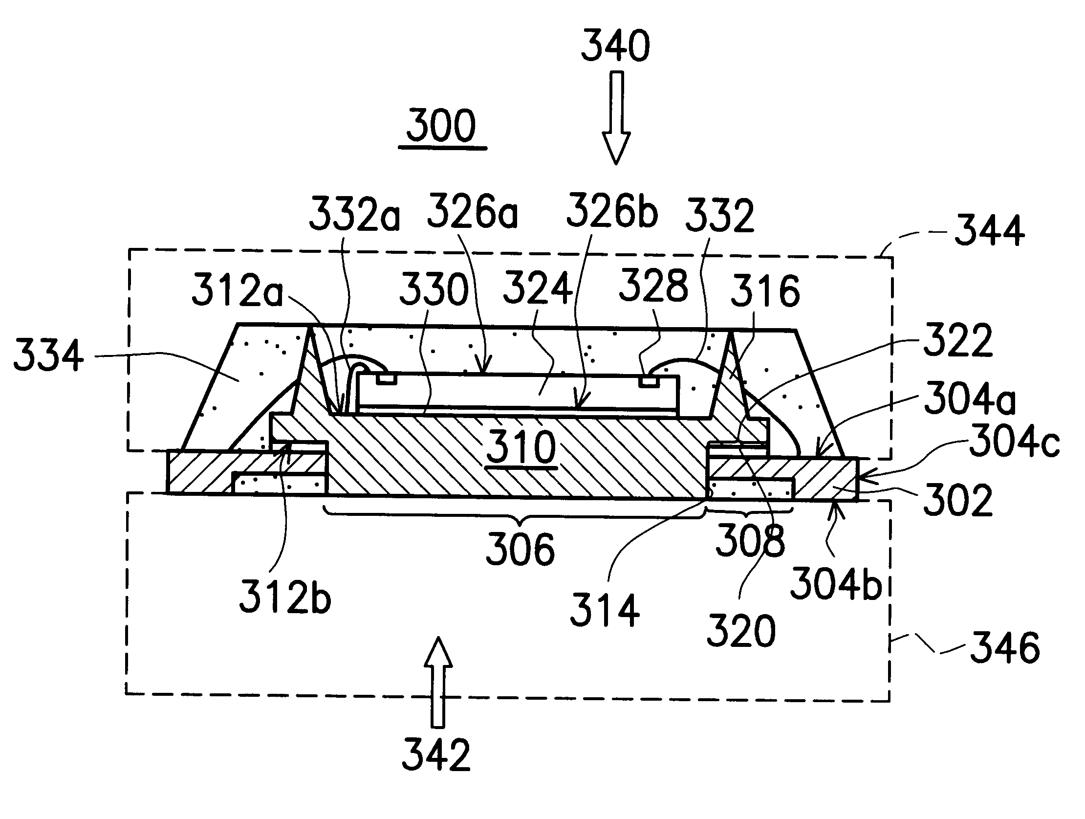
Shown in FIG. 5 is a cross-sectional view of an universal lead frame type of Quad Flat Non-Lead package of a preferred embodiment of the present invention while FIG. 6 is a top view corresponding to FIG. 5 of the present invention. As shown in FIG. 5, and FIG. 6, the lead frame employed by the universal lead flame type of Quad Flat Non-Lead package of the present invention is constituted by a plurality of leads 302 disposed at the perimeter of the chip 324 and surrounding the chip 324. And an opening region 306 is formed at the center of the lead frame. Each of the leads 302 has a first surface 304a (top surface), a second surface 304b (bottom surface), and a side surface 304c. Preferably, the lead 302 is designed to have the second surface 304b form a stepped structure including a relatively thinner protruded region 308 in order to improve the bondability in the subsequent encapsulating process between the leads 302 and the molding compound 334. And the leads 302 preferably extend ...


PUM


Abstract

An universal lead frame type of Quad Flat Non-Lead package of semiconductor comprises a chip, a plurality of leads, a heat sink, and a molding compound. The leads are disposed at the periphery of the chip. The chip has its back surface bonded to the top surface of the heat sink, and the periphery of the top surface of the heat sink has a plurality of projections. The bonding portion at the periphery on the bottom surface of the heat sink is bonded to the top surface of the leads. The protruded portion at the center of the bottom surface of the heat sink is disposed in the opening region such that the bottom surface of the heat sink and the bottom surface of the leads are coplaner. The bonding pads of the chip are electrically connected to the top surface of the leads by a plurality of bonding wires. The molding compound encapsulates the chip, the heat sink, the top surface of the leads, and the bonding wires while exposes the protruded portion of the heat sink.

Description

1. Field of the InventionThis invention relates to a Quad Flat Non-Lead package of semiconductor, and more particularly to a Quad Flat Non-Lead package of semiconductor that can share an universal lead frame to fit various sizes of chip.2. Description of Related ArtFollowing the evolution of the integrated circuit technology, the manufacturing process of integrated circuit has been advanced to ever high in integration with a target of pursuing ever dense package structure in the packaging process of the back end process. The chip scale package (CSP), which has been actively developed and manufactured by the semiconductor industry, has its package size slightly larger than the size of the chip. Therefore, the chip scale package not only can diminish its occupied volume, but also can shorten the path of signal transmission, thereby, it can enhance the product's performance. The carrier employed by the chip scale package includes lead frame, flexible substrate, and rigid substrate etc....

Claims


Application Information

Patent Timeline
IPC IPC(8): H01L21/02H01L23/28H01L21/56H01L23/433H01L23/31H01L23/34
CPCH01L21/565H01L23/3114H01L23/4334H01L24/49H01L2224/48091H01L2224/48247H01L2224/48257H01L2224/49112H01L2224/49171H01L2924/01013H01L2924/01079H01L2924/01082H01L2924/00014H01L24/48H01L2924/01033H01L2924/00H01L2224/45144H01L2224/45124H01L23/49548H01L24/45H01L2224/05554H01L2924/10162H01L2924/14H01L2924/181H01L2924/00012
Inventor HUANG, CHIEN-PINGKO, ERIC
Owner SILICONWARE PRECISION IND CO LTD
Why Eureka
Try Eureka