Floating back gate electrically erasable programmable read-only memory (EEPROM)

Inactive Publication Date: 2001-06-19
GLOBALFOUNDRIES INC
View PDF11 Cites 73 Cited by
  • Summary
  • Abstract
  • Description
  • Claims
  • Application Information

AI Technical Summary

Problems solved by technology

A further problem arises in that, as device sizes shrink, it becomes increasingly difficult to make these memory structures since the injection oxide and the control oxide cannot be shrunk because of charge leakage.
This non-scalability of oxide thickness results in a larger (e.g., longer) electrical distan

Method used


Image

  • Floating back gate electrically erasable programmable read-only memory (EEPROM)
  • Floating back gate electrically erasable programmable read-only memory (EEPROM)
  • Floating back gate electrically erasable programmable read-only memory (EEPROM)

Examples


Embodiment Construction

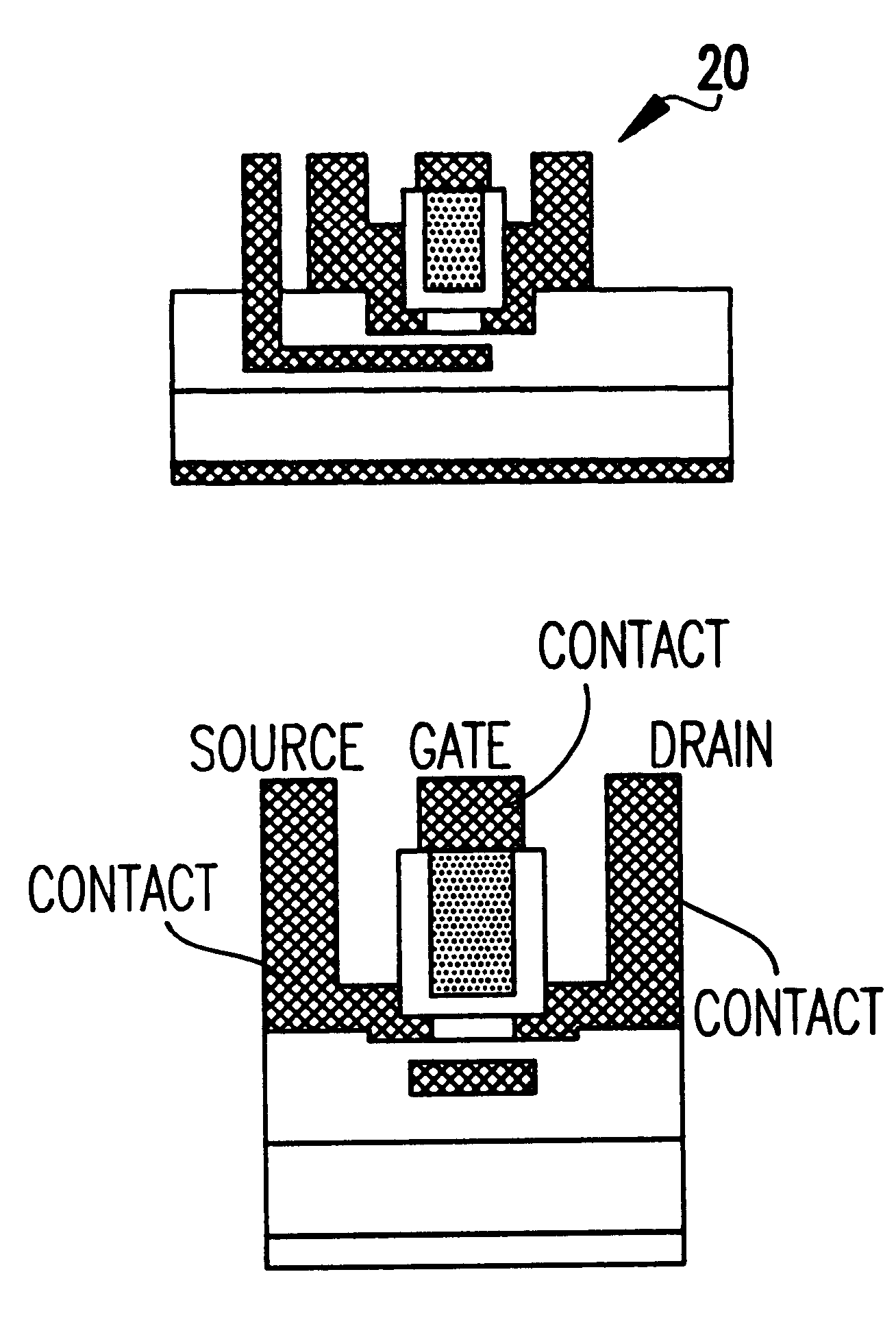
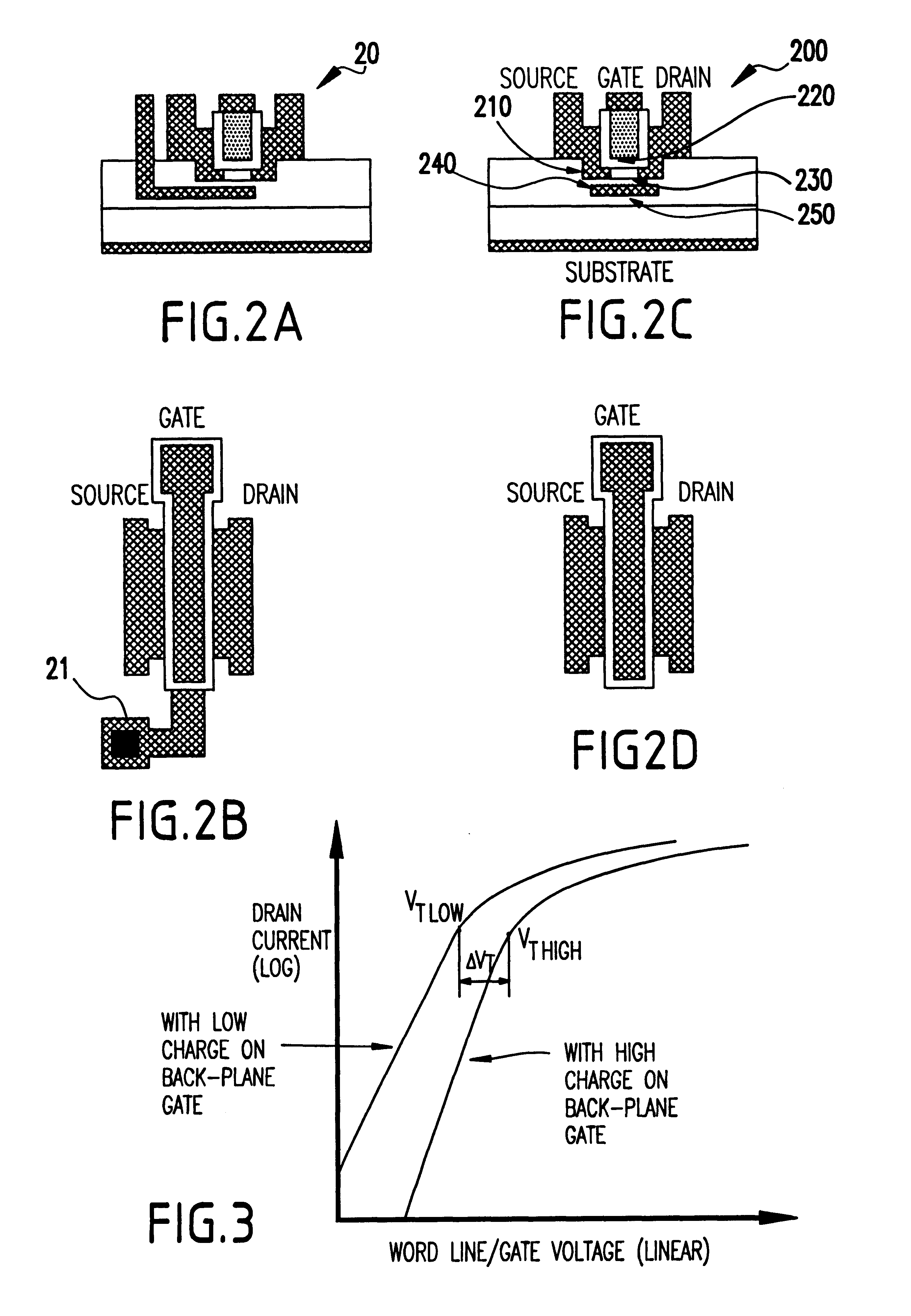
Referring now to the drawings, and more particularly to FIGS. 2(A)-4(F), there is shown a preferred embodiment of the present invention.

As mentioned above, the present invention provides a floating gate memory structure compatible with advanced devices that utilize a buried floating gate, and a method of producing a compact, highly integrated structure which is nonvolatile.

The present inventors have found that achieving acceptable transistor characteristics, as gate lengths are reduced, is made possible by decoupling of the floating gate leakage through the injection / tunnel oxide from that of controlling the transistor channel.

Accordingly, the present invention provides a memory structure in which a back-gate (e.g., a gate formed from a back-plane) serves as a floating gate. This allows the top gate and its oxide to be scalable to requirements originating in the length scaling of the structure.

Typically, back-gates can be larger in size, and hence more efficiently coupled for inject...


PUM


Abstract

A semiconductor memory and a method of producing the memory, includes a transistor including a first gate having an oxide, and a channel, and a back-plane including a second gate and an oxide thereover, the second gate formed opposite to the channel of the transistor, the second gate including a floating gate, wherein a thickness of the oxide of the back-plane is separately scalable from an oxide of the first gate of the transistor.

Description

1. Field of the InventionThe present invention generally relates to a semiconductor device and a method of forming a semiconductor device, and more particularly to a method of forming a semiconductor memory, including a flash memory, and scaling of a memory using a common substrate structure, and to the structure resulting from the inventive method, including a floating gate on a back-plane.2. Description of the Related ArtNon-volatile electrically erasable and programmable memory structures (EEPROMs), such as a flash memory, utilize a floating gate whose charging is controlled by appropriate biasing of the source, drain and controlling gate. A flash memory is unique in providing fast compact storage which is both nonvolatile and rewritable.In a flash memory, the threshold voltage Vt for conduction of a field-effect transistor (FET) changes state depending upon the amount of charge stored in a floating gate (FG) part of the FET. The floating gate is a charge storing region which is ...

Claims


Application Information

Patent Timeline
IPC IPC(8): H01L21/02H01L21/28H01L21/336H01L27/115H01L29/423H01L29/66H01L29/40H01L29/788G11C16/04B82B1/00H01L21/8247H01L29/792
CPCH01L21/28273H01L27/11519H01L27/11521H01L27/1203H01L29/42336H01L29/66825H01L29/7883H01L29/7885H01L29/40114H10B41/10H10B41/30
Inventor KUMAR, ARVINDTIWARI, SANDIP
Owner GLOBALFOUNDRIES INC
Why Eureka
Try Eureka