One time programmable read-only memory comprised of fuse and two selection transistors

a read-only memory and fuse technology, applied in the field of one time programmable read-only memory, can solve the problems of unnecessarily large cell size of the conventional otprom, thickness complicating the process of fabricating the conventional otprom, etc., and achieves a simple and simple process for fabricating.

Inactive Publication Date: 2006-09-14
LEADIS TECH
View PDF5 Cites 46 Cited by
  • Summary
  • Abstract
  • Description
  • Claims
  • Application Information

AI Technical Summary

Benefits of technology

[0015] To select the memory cell and destroy the fuse during a write operation to the OTPROM, a first voltage, a second voltage, and a third voltage are applied to the fuse electrode of the fuse, the gate electrode of the first transistor, and the gate electrode of the second transistor, respectively, where the first voltage is higher than a threshold breakdown voltage of the fuse insulation layer of the fuse and the second voltage and the third voltage are lower than the first voltage. In one embodiment, the third voltage is substantially same as the second voltage. In another embodiment, the second voltage and the third voltage are substantially half of the first voltage. Note that the difference between the first voltage and the second voltage is set lower than the threshold breakdown voltage of the gate insulation layer of the first transistor, so that the gate insulation layer of the first transistor in an unselected memory cell is not destroyed during the write operation to the selected memory cell connected to the unselected memory cell.
[0020] The OTPROM of the present invention has the advantage that the OTPROM structure is simple with the thickness of the gate insulation layer of the selection transistors being substantially same as that of the fuse insulation layer. This results in a much simpler process for fabricating the OTPROM, because misalignment margins need not be added in the fabrication process.

Problems solved by technology

However, having a gate insulation layer 12 and a fuse insulation layer 10 with different thicknesses complicates the process for fabricating the conventional OTPROM, as will be clear from FIGS. 3A-3H.
This results in an unnecessarily large cell size for the conventional OTPROM.
Note that this disadvantage of the conventional OTPROM is caused by the requirement that the gate insulation layer 12 should be thicker than the fuse insulation layer 10 in conventional OTPROMs to prevent the gate insulation layer 12 from also being destroyed when the fuse insulation layer 10 is destroyed, in response to a voltage Vcc high enough to destroy the fuse 11.

Method used


Image

  • One time programmable read-only memory comprised of fuse and two selection transistors
  • One time programmable read-only memory comprised of fuse and two selection transistors
  • One time programmable read-only memory comprised of fuse and two selection transistors

Examples


Embodiment Construction

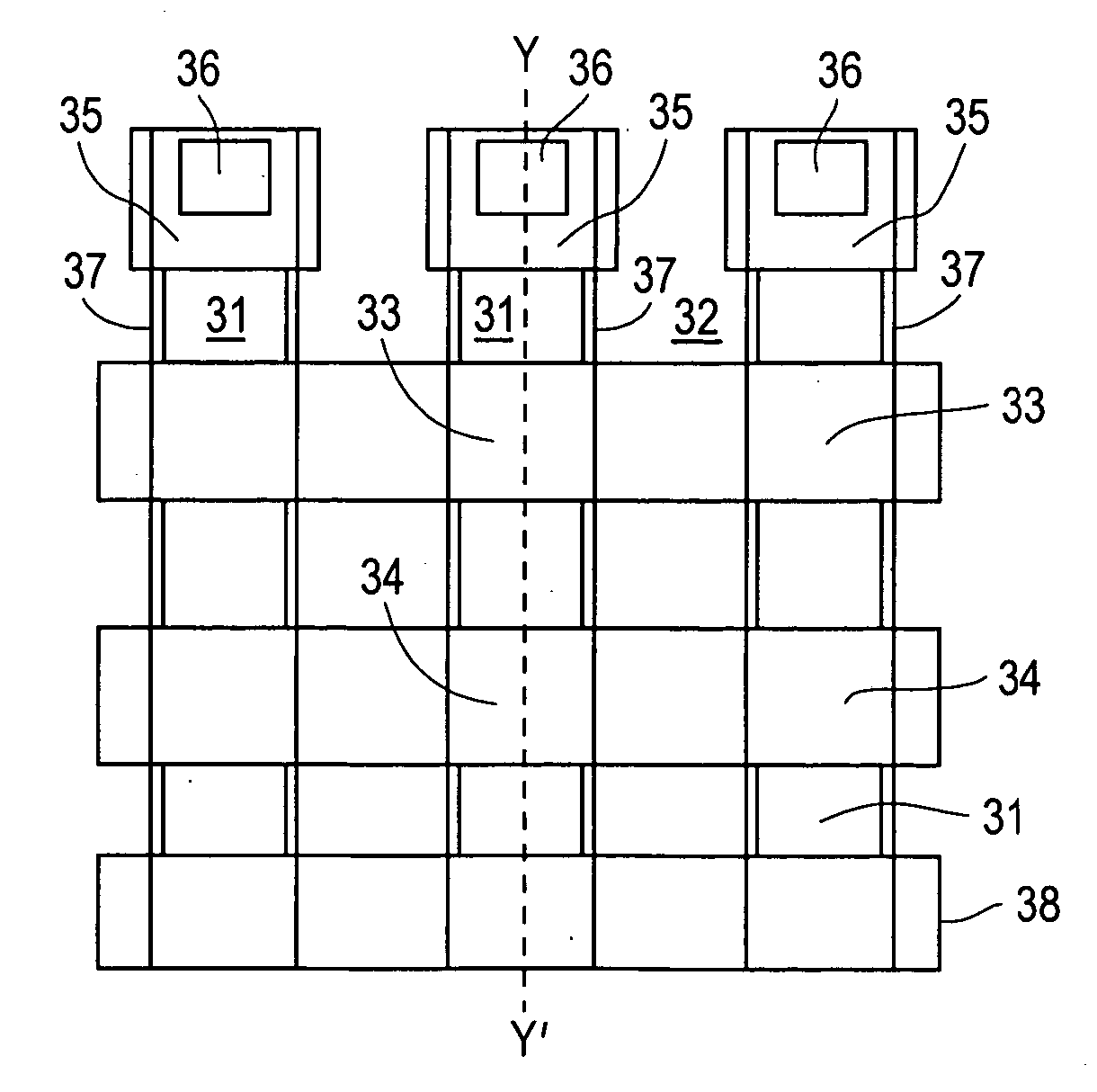
[0034]FIG. 4 is a top view of the layout of an OTPROM device formed on a semiconductor wafer, according to one embodiment of the present invention, and FIG. 5 is a cross-sectional view of the semiconductor wafer of a memory cell of the OTPROM device across the line Y-Y′ of FIG. 4, according to one embodiment of the present invention. Referring to FIGS. 4 and 5, the memory cells of the OTPROM are formed on the active regions 31 longitudinally formed on the substrate 41. The active regions 31 are separated by field regions 32 longitudinally formed between the active regions 31.

[0035] Each memory cell of the OTPROM includes a fuse 100, a first selection transistor 102, and a second selection transistor 104. The fuse 100 is comprised of a buried junction layer 40, an insulation layer 61, and a fuse electrode 35. The fuse electrode 35 is located at one end of the active region 31. The first selection transistor 102 is comprised of a drain region 63, a source region 62, the gate insulati...


PUM


Abstract

A one time programmable read-only memory (OTPROM) device includes a plurality of memory cells, where a memory cell of the OTPROM device comprises a fuse indicating a first memory state of the memory cell if the fuse is destroyed and a second memory state of the memory cell if the fuse is not destroyed, a first transistor coupled to the fuse, and a second transistor serially coupled to the first transistor. Both the first transistor and the second transistor are turned on to select the memory cell, and at least one of the first transistor and the second transistor are turned off to unselect the memory cell. The fuse insulation layer of the fuse and the gate insulation layers of the first and second transistors share a common insulation layer formed in the same fabrication process.

Description

TECHNICAL FIELD [0001] The present invention relates to a one time programmable read-only memory (OTPROM) and, more specifically, to an OTPROM including memory cells each comprised of a fuse and two serially connected selection transistors and methods of operating and fabricating such OTPROM. BACKGROUND OF THE INVENTION [0002] OTPROMs are semiconductor storage devices that can be programmed or written only once. OTPROMs are similar to erasable programmable read-only memories (EPROMs) in that they can be programmed, but are different from EPROMs in that OTPROMs have no means for erasing the stored content while the content stored in EPROMs can be erased with ultraviolet through a quart glass window in the EPROMs. OTPROMS are widely used where smaller package size is needed. [0003]FIG. 1 is a top view of the layout of a conventional OTPROM device formed on a semiconductor wafer, and FIG. 2 is a cross-sectional view of the semiconductor wafer of a memory cell of a conventional OTPROM d...

Claims


Application Information

Patent Timeline
Patent Type & Authority Applications(United States)
IPC IPC(8): G11C17/18
CPCG11C17/16H01L27/112H01L27/11206H10B20/20H10B20/00
Inventor LEE, DONG KYU
Owner LEADIS TECH
Why Eureka
Try Eureka