Mechanical fixture for holding electronic devices under test showing adjustments in multiple degrees of freedom

a technology of electronic devices and mechanical fixtures, which is applied in the direction of workpiece holders, manufacturing tools, instruments, etc., can solve the problems of limiting factors, affecting the accuracy of the placement of the probe in an adjacent set of i/o points, and physical mechanical limitations of the probes

Inactive Publication Date: 2001-07-17
IBM CORP
View PDF18 Cites 29 Cited by
  • Summary
  • Abstract
  • Description
  • Claims
  • Application Information

AI Technical Summary

Problems solved by technology

However, as the density of the I/O increases, the physical mechanical limitations of the probes beco...

Method used


Image

  • Mechanical fixture for holding electronic devices under test showing adjustments in multiple degrees of freedom
  • Mechanical fixture for holding electronic devices under test showing adjustments in multiple degrees of freedom
  • Mechanical fixture for holding electronic devices under test showing adjustments in multiple degrees of freedom

Examples


Embodiment Construction

However, it should be understood that these embodiments are only examples of the many advantageous uses of the innovative teachings herein. In general, statements made in the specification of the present application do not necessarily limit any of the various claimed inventions. Moreover, some statements may apply to some inventive features but not to others. In general, unless otherwise indicated, singular elements may be in the plural and vice versa with no loss of generality.

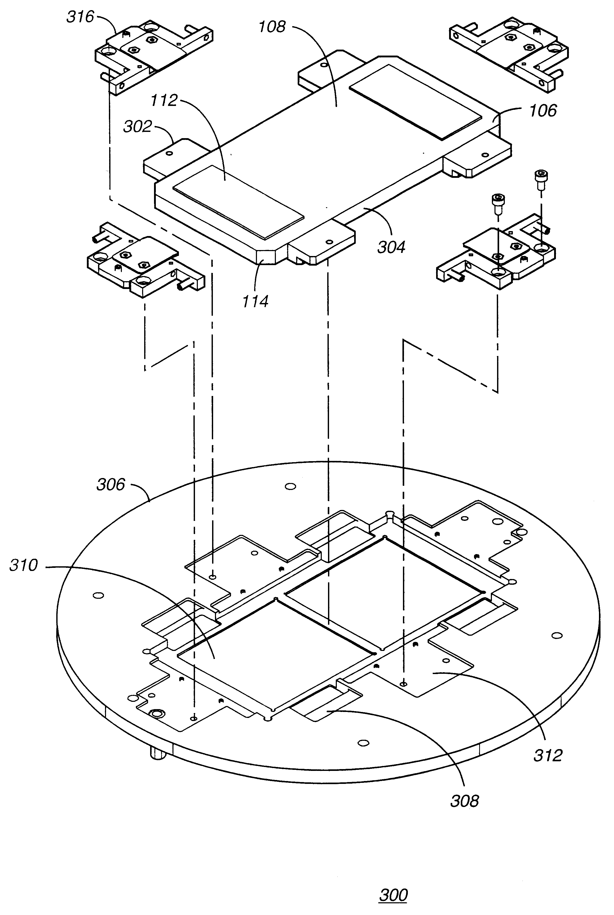
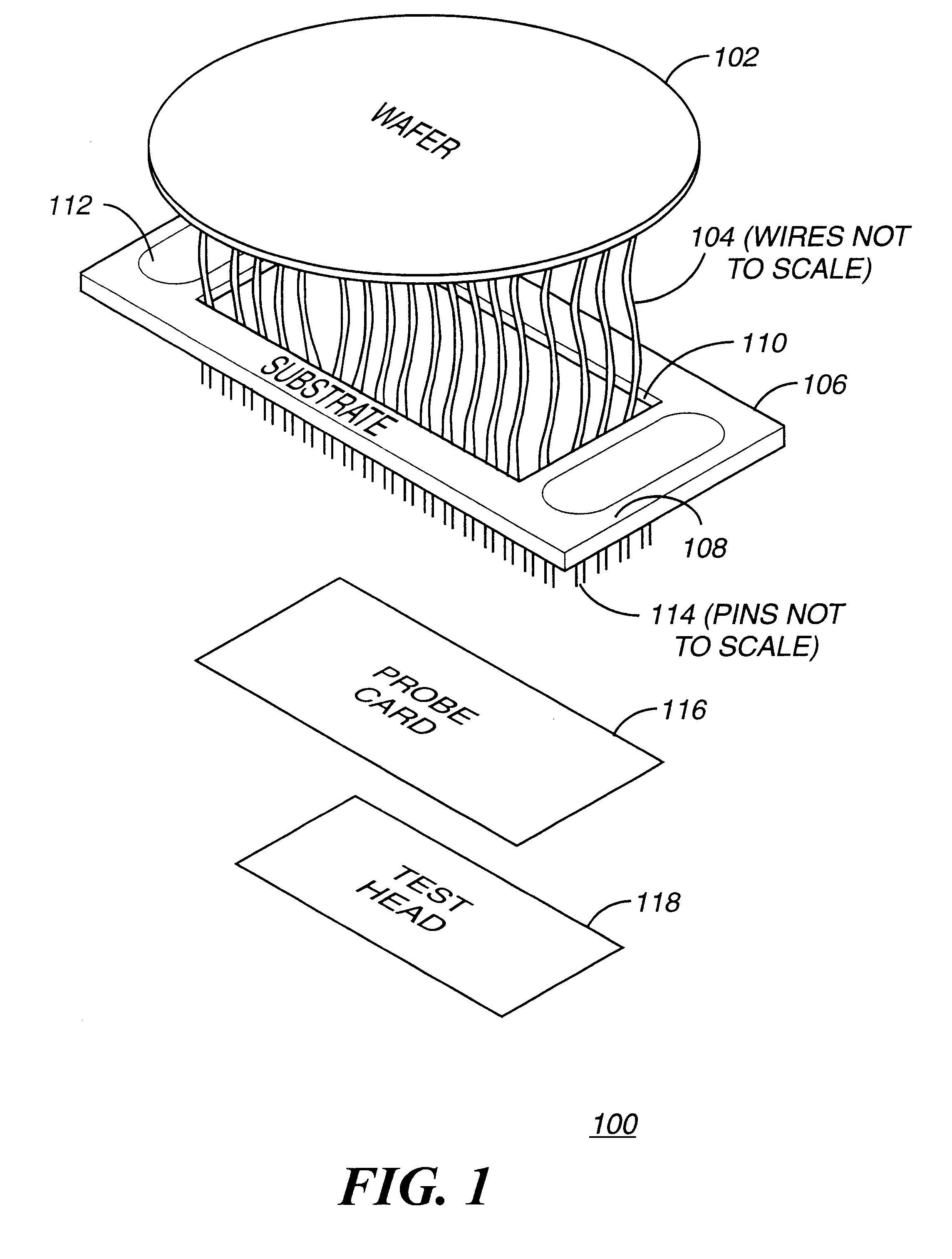
Referring now in more detail to the drawings in which like numerals refer to like parts throughout several views, as described in FIG. 1, the device (not shown) to be tested on a semiconductor wafer 102 is electrically coupled via wires 104 to a substrate 106 with probe areas 118 fan out electrical signals from the wafer I / O. The substrate 106 is a multilayer substrate, such as a ceramic substrate with one or more layers of metalization. The substrate 106 has a contact area 110 for electrically coupling with ...


PUM


Abstract

A fixture to hold an electronic substrate having probe areas on a top surface. The top surface of the electronic substrate is left open to provide a maximum area to couple interconnect wires for a device under test. In addition, a bottom surface of the substrate is left open to provide a maximum area to couple with a probe card in one embodiment, or a test head in another embodiment. This open bottom and open top minimize the mechanical interference with electrical connections. The substrate is planarized to a frame by one or more clamps that are attached to the frame. The clamps provide adjustment of the pressure down on the substrate in a Z-axis direction which is normal to the top surface of the substrate for providing a good connection with a planar card. In addition, the clamps provide adjustment in the an X-Y plane parallel to the frame and rotational correction about the Z-axis.

Description

Not Applicable1. Field of the InventionThe invention relates to the mechanical fixtures for holding electronic devices under test, and more particularly the present invention relates to a mechanical fixture that can adjust the device being held in X, Y, Z and theta (.THETA.) direction while accommodating several hundred of pounds of force in the Z-direction.2. Description of the Related ArtThe density of semiconductor electronics increases every year. One known postulate in the field of semiconductor manufacturing is Moore's Law which predicts every 18 months the density of semiconductor circuitry doubles. Besides the obvious decrease in size for semiconductor devices, the number of transistors or gates that can be offered in a given die size continues to grow. This increase density allows for more complex circuitry to be eveloped. And although the increase in semiconductor density is very desirable it is not without its shortcomings.One shortcoming is the increase in the density of...

Claims


Application Information

Patent Timeline
IPC IPC(8): G01R31/28
CPCG01R31/2887Y10S269/90Y10S269/903
Inventor BARRINGER, DENNIS R.LAFORCE, MARK R.MARNELL, MARK A.PORTER, DONALD W.SCHMIDT, ROGER R.WHITE, WADE H.
Owner IBM CORP
Why Eureka
Try Eureka