Method for dual damascene process using electron beam and ion implantation cure methods for low dielectric constant materials

a dielectric constant, electron beam technology, applied in the direction of basic electric elements, electrical equipment, semiconductor devices, etc., can solve the problems of reduced surface wiring space, reduced yield, and high cost of multi-level metal systems

Inactive Publication Date: 2001-08-07
NEWPORT FAB
View PDF6 Cites 118 Cited by
  • Summary
  • Abstract
  • Description
  • Claims
  • Application Information

AI Technical Summary

Problems solved by technology

As more and more circuit components are placed on the wafer surface, the amount of space available for surface wiring decreases.
Multi level metal systems are more costly and have lower yields.
In the past, the primary metallization material used in semiconductor fabrication was aluminum due to the leakage and adhesion problems experienced with the use of gold and the high contact resistance with silicon experienced with copper.
However, over time, the semiconductor industry has slowly been moving to the use of copper for metallization due to the alloying and electromigration problems that are seen with aluminum.
Further, since the industry is moving to prefer copper over aluminum for metallization, the damascene process is even more important in that copper is extremely difficult to etch.
However, due to the risks and expenses associated with incorporating all three large scale trends in manufacturing semiconductor devices, many believe that industry competitors will likely implement only one or two of these changes in fabricating semiconductor devices.

Method used


Image

  • Method for dual damascene process using electron beam and ion implantation cure methods for low dielectric constant materials
  • Method for dual damascene process using electron beam and ion implantation cure methods for low dielectric constant materials
  • Method for dual damascene process using electron beam and ion implantation cure methods for low dielectric constant materials

Examples


Embodiment Construction

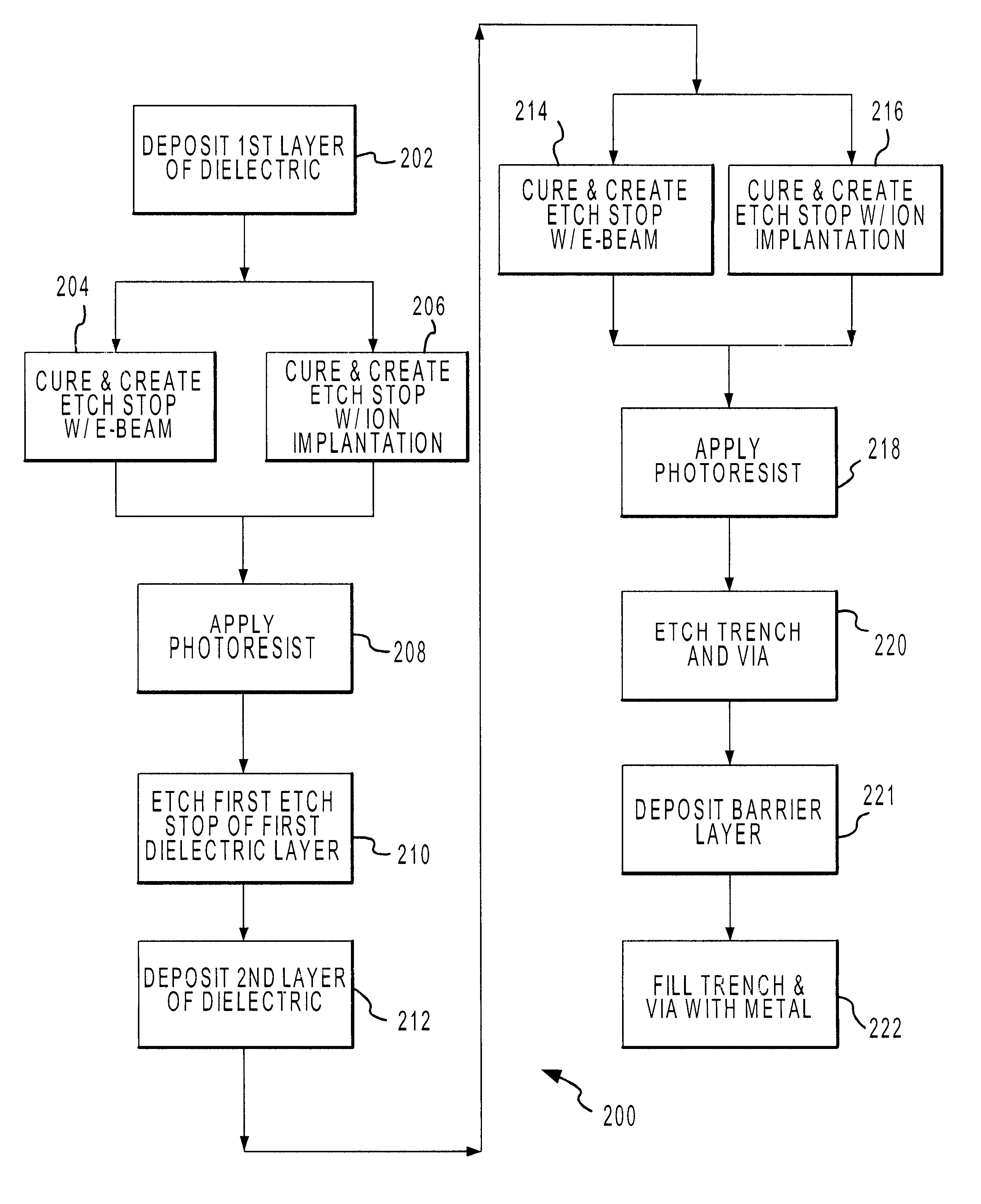
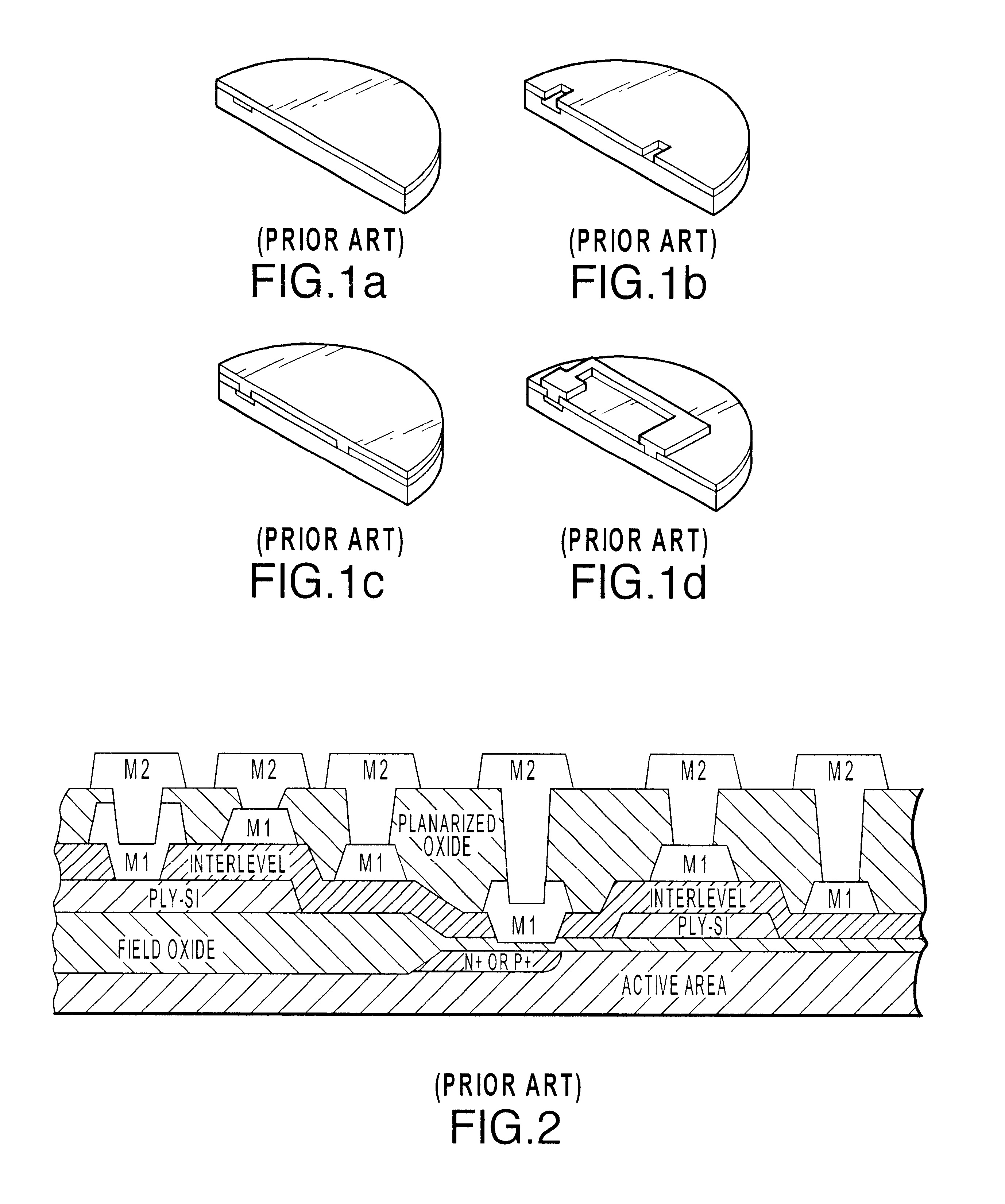
As the semiconductor industry moves to smaller and smaller integrated circuit features, the aspect ratio of the interconnects connecting these features increases and it becomes more and more difficult to obtain good etching and good gap fill results. Accordingly, metal etch and dielectric gap fill are seen as the industry's greatest challenges in moving to smaller dimensions. Damascene processing eliminates both of these conventional steps used in processing interconnects and, as a result, the industry has moved toward improving damascene processing techniques.

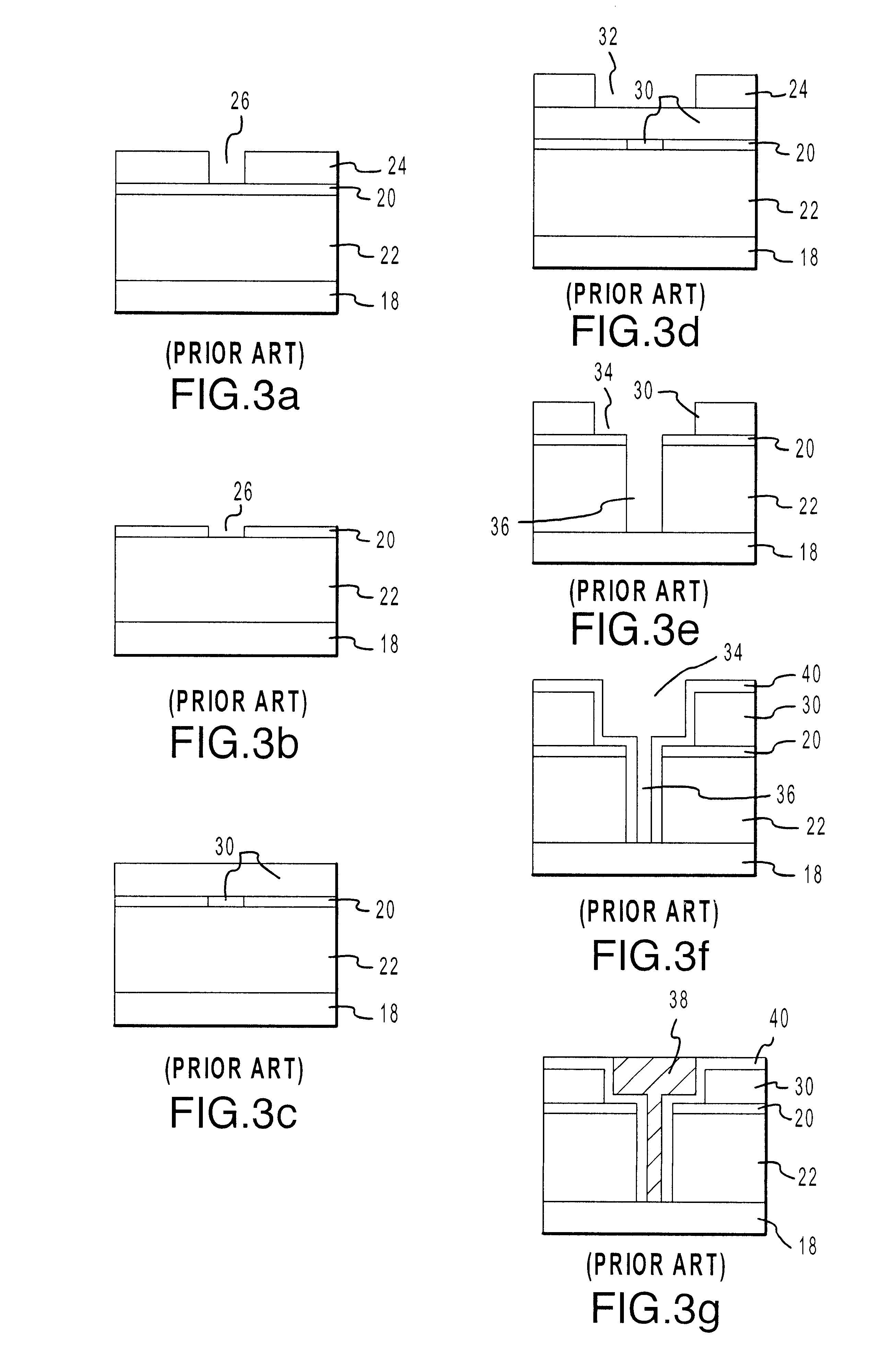
The steps involved in an exemplary prior art dual damascene metallization process are shown in FIGS. 3a-3f. The process typically begins with a silicon wafer substrate that is covered with an insulator layer. The insulator is typically a dielectric, and preferably a material having a low dielectric constant. Masking then takes place to create patterns for the via and trench, and an etch stop layer such as a thin silicon nitrid...


PUM


Abstract

Method for dual damascene metallization of semiconductor workpieces which uses a process for creating an etch stop in an insulator thereby eliminating the need for deposition of an etch stop layer. Electron beam exposure is used to cure the insulator, or material having a low dielectric constant. Application of the electron beam to the low dielectric constant material converts the topmost layer of the low dielectric constant material to an etch stop layer, while rapid thermal heating cures the remainder of the low dielectric constant material. Creation of an etch stop layer in the low dielectric constant material can also be achieved by curing the low dielectric constant material using ion implantation.

Description

1. Technical FieldThe present invention relates, generally, to dual damascene processing and, more particularly, to a method for dual damascene processing using electron beam and ion implantation cure methods for a material having a low dielectric constant.2. Background Art and Technical ProblemsMetallization, which generally refers to the materials, methods and processes of wiring together or interconnecting the component parts of an integrated circuit located on the surface of a wafer, is critical to the operation of semiconductor devices. As shown in FIGS. 1a through 1d, the conventional metallization process for a single layer metal system used in fabricating semiconductor devices first involves contact masking which is the etching of contact holes or "contacts" through all the surface layers on a semiconductor device until contact is made with the active regions of the device as shown in FIG. 1b. Next, as shown in FIG. 1c, a thin layer of the conducting metal is deposited over ...

Claims


Application Information

Patent Timeline
Patent Type & Authority Patents(United States)
IPC IPC(8): H01L21/768H01L21/70
CPCH01L21/7681H01L21/76811H01L21/76829H01L21/76825Y10S438/949
Inventor LIU, QIZHIFEILER, DAVIDZHAO, BINBRONGO, MAUREEN R.
Owner NEWPORT FAB
Why Eureka
Try Eureka