Fabrication of sub-micron etch-resistant metal/semiconductor structures using resistless electron beam lithography

a technology of electron beam lithography and metal/semiconductor, which is applied in the direction of photomechanical equipment, instruments, originals for photomechanical treatment, etc., can solve the problems of inconvenient operation, inconvenient use, and inability to meet the requirements of the lithographic process

Inactive Publication Date: 2001-07-17
SCOPRA SCI & GENIE SEC
View PDF22 Cites 37 Cited by
  • Summary
  • Abstract
  • Description
  • Claims
  • Application Information

AI Technical Summary

Benefits of technology

The use of a focused electron beam in a resistless lithography method enables the production of a structure of etch-resistant metal / semiconductor compound having linewidths as thin as 50 nm.

Problems solved by technology

These types of lithographic processes suffer from several limitations which can become extremely constraining in the fabrication of sub-100 nm devices.
These limitations include undesirable proximity effects in the resist and resolution limits imposed by the size of the polymer molecules.
These high energy electrons expose the resist in an undesirable region.
However, none of these techniques are intended as lithography processes or for the fabrication of masks for lithography.
However, the wavelength of ultra-violet light represents a physical limit to the resolution that can be achieved using this technique.
A major challenge in the fabrication of these masks is to use electron-beam lithography to form structures (etch masks) that have both a high resolution and an excellent resistance to chemicals employed to remove the absorbent layer of heavy atoms in unprotected regions.
Conventional techniques using polymeric resists as etch masks either do not provide a sufficient resolution or do not provide a sufficient resistance to chemical etching (J. P. Silverman, Journal of Vacuum Science and Technology, B15, 2117 (1997)).

Method used


Image

  • Fabrication of sub-micron etch-resistant metal/semiconductor structures using resistless electron beam lithography
  • Fabrication of sub-micron etch-resistant metal/semiconductor structures using resistless electron beam lithography
  • Fabrication of sub-micron etch-resistant metal/semiconductor structures using resistless electron beam lithography

Examples


example 2

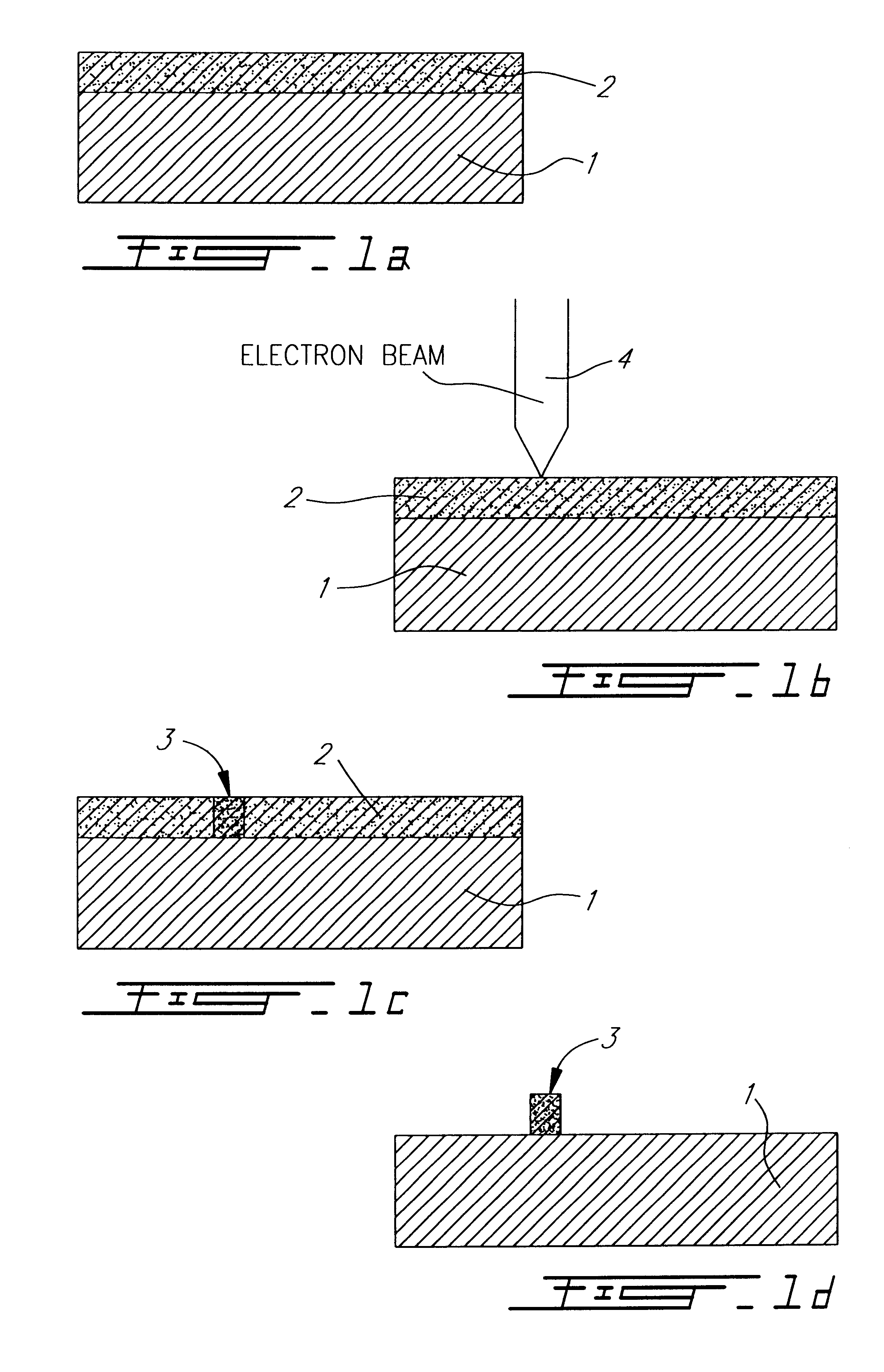
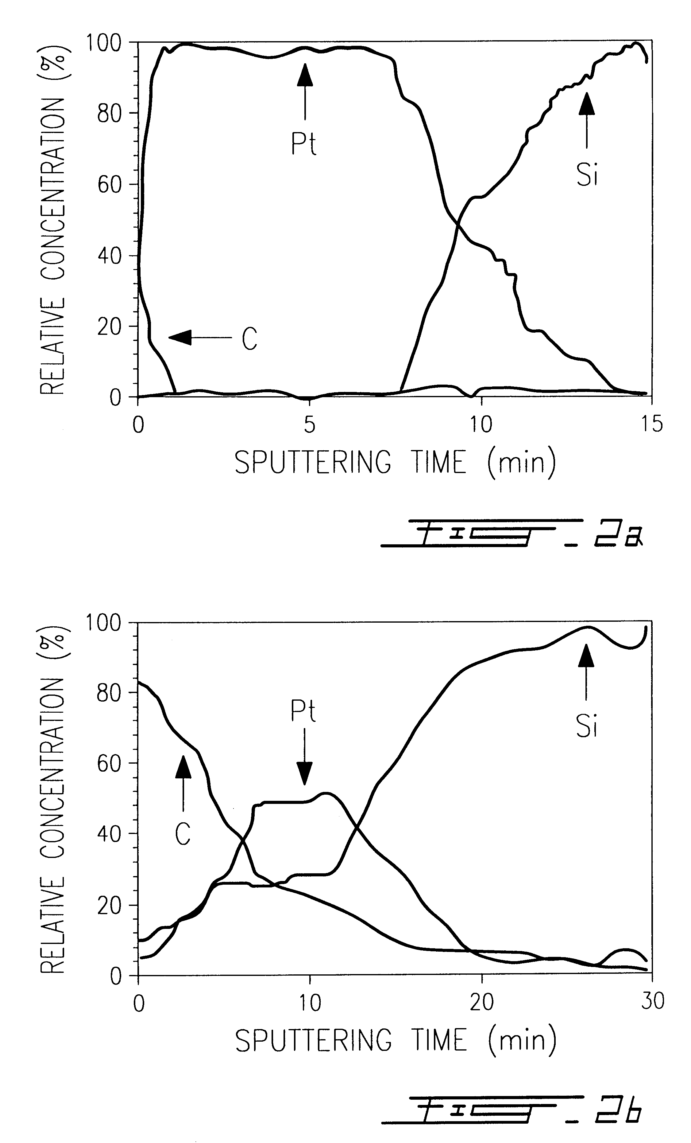
As an example to form fine structures using 20 nm of Pt evaporated on a silicon substrate, a 3 keV electron beam would be adequate. In fact linewidths less than 50 nm have been obtained using a 100 pA electron beam (.apprxeq.200 mA / cm.sup.2), 1.5 .mu.C / cm dose. In this case, to reduce the carbon contamination and the local charging effects, the complete dose was achieved by multiple exposition (J. Fujita, H. Watanabe, Y. Ochiai, S. Manako, J. S. Tsai and S. Matsui, Appl. Phys. Lett., 66, 3065 (1995)). More specifically, each segment of the microstructure has been exposed 20 times using a reduced line dose of 0.075 .mu.C / cm. The effect of carbon contamination is to absorb some of the electron energy, thus reducing the amount of energy lost in the metal layer and decreasing the temperature rise. This technique of multiple exposition reduces the total line dose required for threshold, by reducing the rate of carbon deposition. Multiple repetition also significantly decreases the linewi...

example 3

The details of the method presented in this example will emphasize the particular case of fabrication of masks for X-ray lithography using a platinum silicide. The activation energy to form the first type of platinum silicide (Pt.sub.2 Si) is around 1.4 eV and the temperature range for a complete transformation of Pt into Pt.sub.6 Si is from 200-350.degree. C. [Colgan, E. G, Journal of Material Resistance, 10, 1953, (1995)]. A focused electron beam of a standard scanning electron microscope (SEM) at low energy (1 to 3 keV) provides sufficient energy to locally form this silicide, despite the heat dissipation in the material.

A tantalum layer of 450 nm was evaporated onto a clean X-ray transparent material (glass) using an electron gun deposition system. Using the same deposition system, a 40 nm layer of silicon and a 20 nm layer of platinum are deposited in sequence. The electron beam lithography system consists of a JEOL JSM-6300 scanning electron microscope (SEM) equipped with a tu...

example 4

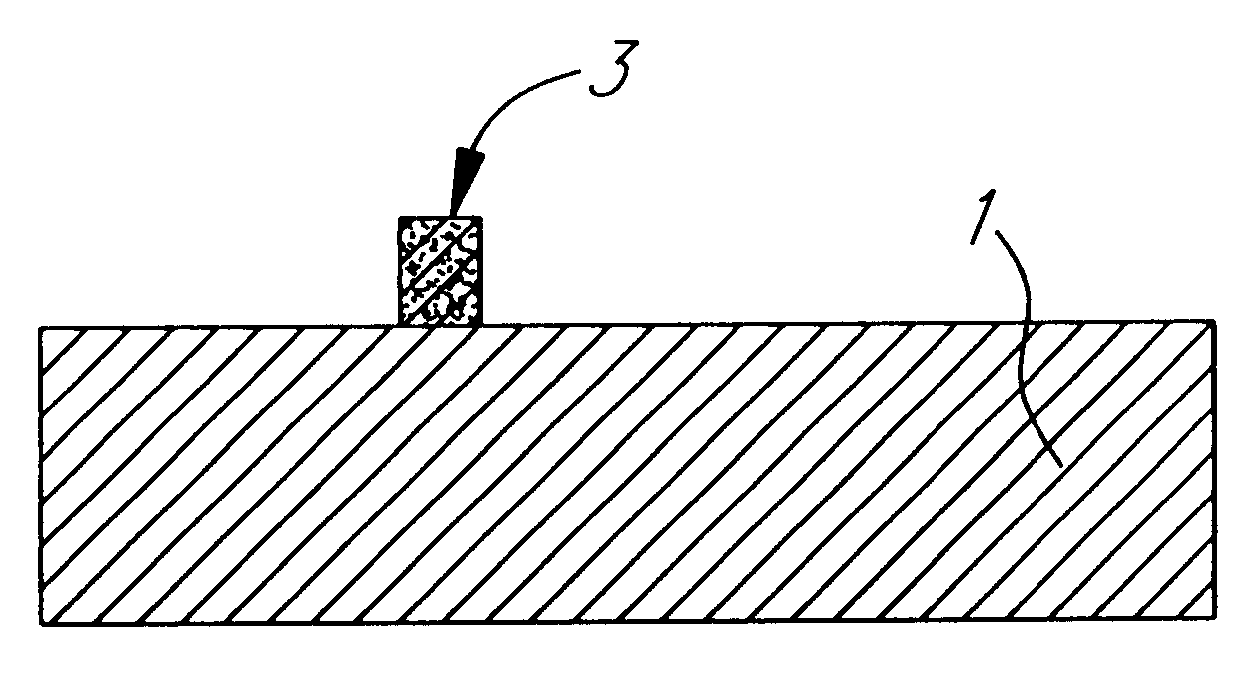
Another example of the method is the fabrication of molds for nanoimprint lithography. These molds need to be resistant to mechanical constraints that are applied to transfer the pattern from the mold to a mechanically impressible surface. The fabrication of molds requires an etch mask which has both high resolution and excellent resistance to the chemicals used to etch the mold substrate. With our technique, a mechanically resistant substrate (such as tantalum or silicon carbide) is covered by a thin layer of silicon, followed by a thin layer of a metal able to form silicide. The electron beam lithography system transfers the pattern by forming silicide regions on the surface. Wet etching in a strong acid is used to remove the thin metal layer in unexposed regions. Similarly, a plasma etch or a wet etch can be used to remove the thin silicon layer in unexposed regions. A reactive ion etcher or any directional etching process can then be used to etch the substrate. Exposed regions o...


PUM

PropertyMeasurementUnit
temperatureaaaaaaaaaa

Abstract

A method for fabricating a sub-micron structure of etch-resistant metal / semiconductor compound on a substrate of semiconductor material comprises the step of depositing onto the substrate a layer of metal capable of reacting with the semiconductor material to form etch-resistant metal / semiconductor compound, and the step of producing a focused electron beam. The focused electron beam is applied to the layer of metal to locally heat the metal and semiconductor material and cause diffusion of the metal and semiconductor material in each other to form etch-resistant metal / semiconductor compound. The focused electron beam is displaced onto the layer of metal to form the structure of etch-resistant metal / semiconductor compound. Finally, the layer of metal is wet etched to leave on the substrate only the structure of metal / semiconductor compound. Following wet etching of the layer of metal, an oxygen plasma etch can be conducted to remove a carbon deposit formed at the surface of the structure of etch-resistant metal / semiconductor compound. Also, the substrate may be subsequently etched to remove a thin layer of metal rich semiconductor material formed at the surface of the substrate by reaction, at room temperature, of the metal and semiconductor material with each other.

Description

1. Field of the InventionThe present invention relates to a method for fabricating a structure of etch-resistant metal / semiconductor compound using resistless electron beam lithography, more specifically a highly focused electron beam to produce a sub-micron structure of etch-resistant metal / semiconductor compound.2. Brief Description of the Prior ArtThe fabrication of ultra-small scale electronic devices requires efficient high resolution lithography techniques. Resist-based lithography processes are very frequently involved in these high resolution lithography techniques, and poly(methyl methacrylate) (PMMA) is the polymer most widely used as a resist for electron beam lithography applications (S. P. Beaumont, P. G. Bower, T. Tamamura, C. D. W. Wilkinson, Appl. Phys. Lett., 38, 438 (1991) and W. Chen, H. Ohmed, J. Vac. Sci. Technol., B 11, 2519 (1993)).These types of lithographic processes suffer from several limitations which can become extremely constraining in the fabrication o...

Claims


Application Information

Patent Timeline
Patent Type & Authority Patents(United States)
IPC IPC(8): H01L21/44H01L21/02G03F1/00G03F1/24G03F1/58G03F1/68G03F7/00G03F7/20G03F9/02H01L21/027H01L21/30
CPCB82Y10/00B82Y40/00G03F1/14G03F1/58G03F1/68G03F7/0002G03F1/24G03F7/2059G03F1/78H01L21/027
Inventor BEAUVAIS, JACQUESDROUIN, DOMINIQUELAVALLEE, ERIC
Owner SCOPRA SCI & GENIE SEC
Why Eureka
Try Eureka