Method of making nanopatterns and nanostructures and nanopatterned functional oxide materials

a functional oxide and nano-structure technology, applied in the field of making nano-structured functional oxide materials, can solve the problems of difficult etching of such materials, limited technique for ceramic patterns under 100 nm resolution, and inability to achieve true nanometer-scale patterning resolution. achieve the effect of higher patterning speed

Inactive Publication Date: 2008-03-20
NORTHWESTERN UNIV
View PDF3 Cites 37 Cited by
  • Summary
  • Abstract
  • Description
  • Claims
  • Application Information

AI Technical Summary

Benefits of technology

[0015] The invention provides a versatile nanopatterning method suitable for a broad range of material-substrate systems. The types of materials that can be patterned seem to be limited only by the availability of appropriate liquid precursors that are compatible with electron beam sensitive resists. Use of highly sensitive electron beam resists for patterning provides higher patterning speeds. In addition, spin coating is not only a low-cost process but also a high-throughput process. The method permits nanopatterning of inorganic materials and organic materials on a variety of substrates to form nanopatterns and / or nanostructures with control of dimensions and location without the need for etching the materials and without the need for realignment between multiple patterning steps in forming nanostructures, such as heterostructures comprising multiple materials.

Problems solved by technology

Although several nanopatterning schemes have been developed during the last two decades, techniques that can pattern ceramics under 100-nm resolution are very limited.
This is due in part to the refractory nature of ceramics and the difficulty in etching such materials.
Although this technique was shown to generate very fine structures (<10 nm), it is limited to resists that are sensitive to e-beams and the process typically requires a high electron dose for development of e-beam-sensitive inorganic resists.
However, these techniques do not attain true nanometer-scale patterning resolution.
The key bottleneck is the stringent requirement on feature realignment between the multiple patterning steps, which are required in order to form nonplanar patterns composed of more than two materials.
However they are demonstrated mainly for metals and polymers, and are not well suited for ceramics.
Direct deposition methods such as robotic deposition enable the fabrication of intricate ceramic structures, yet there are restrictions on the deposition environment and the smallest feature size attainable.

Method used


Image

  • Method of making nanopatterns and nanostructures and nanopatterned functional oxide materials
  • Method of making nanopatterns and nanostructures and nanopatterned functional oxide materials
  • Method of making nanopatterns and nanostructures and nanopatterned functional oxide materials

Examples


example 1

[0037] To demonstrate the capabilities of an illustrative method, liquid precursors of technologically important inorganic ceramic oxides ZnO and PZT were evaluated. The liquid ZnO precursor was prepared using chemicals purchased from Sigma-Aldrich Inc. and used in as-received form without further purification. In a typical process, zinc oxide sol is prepared by stirring a mixture of zinc acetate dihydrate, 2-methoxy ethanol, and ethanol amine at 60° C. for 2 hr. The relative compositions were adjusted to give a 0.1 M ZnO sol with equimolar ratio of zinc and ethanol amine. This sol is transparent and remains stable for more than a year.

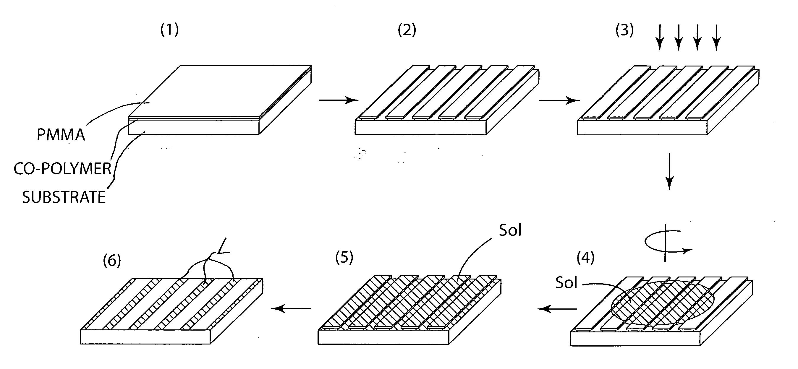
[0038] Referring to FIG. 1, illustrative steps in nanopatterning pursuant to a method embodiment of the invention are shown schematically. The first step (1) is to sequentially spin-coat a surface-oxidized Si substrate (Siox / Si) with a bilayer structure of electron beam (eb) sensitive resists with a relatively higher eb sensitive MMA-MAA copolymer re...

example 2

[0043] This example is provided to illustrate that an organic material can be patterned using a dilute solution of polypyrrole, a popular conducting polymer, on a SiOx / Si substrate surface. Polypyrrole in 3% water was received as a black solution with proprietary organic acids from Sigma-Aldrich Inc. This solution was further diluted to a 1:3 ratio of polypyrrole to water and was used for patterning polypyrrole patterns with different line widths and spacing, FIG. 3. The method steps were the same as those described with respect to EXAMPLE 1.

example 3

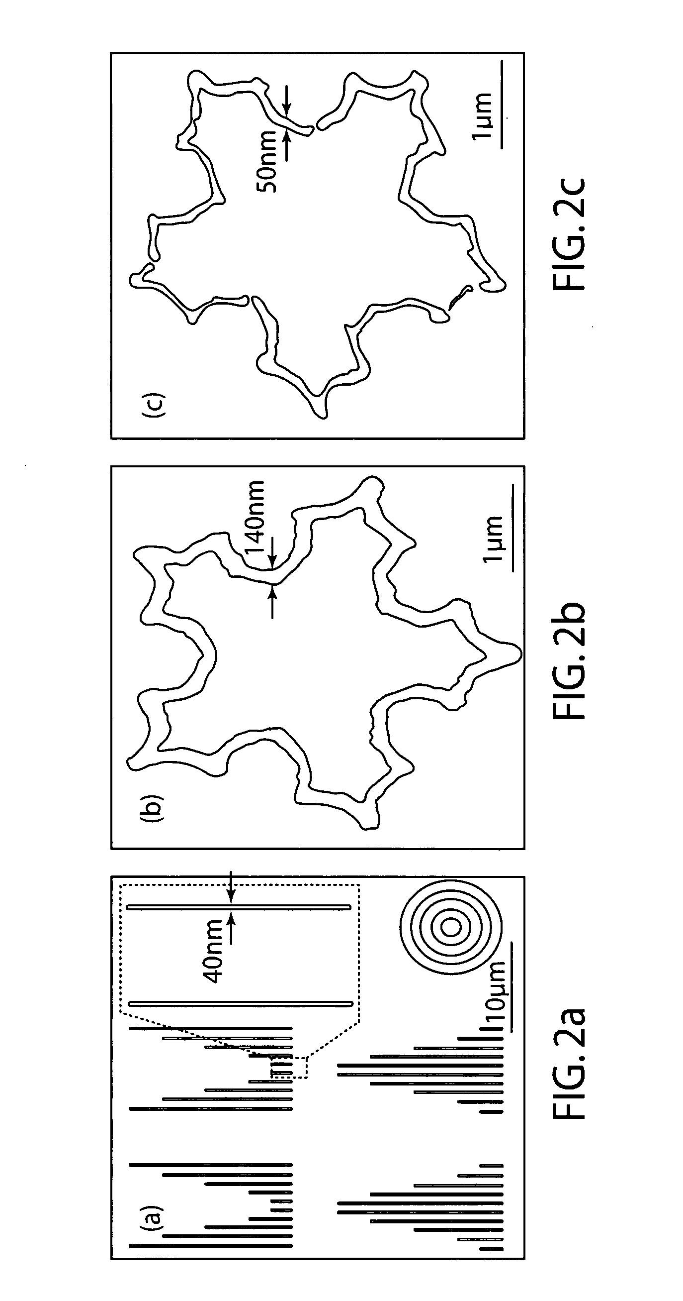
[0044] This example demonstrates that the above method embodiment can be practiced to nanopattern diverse material systems with a variety of substrates. For example, FIG. 4a shows a PZT ring structure having a wall thickness of 80 nm patterned on a Pt / Ti / SiOx / Si substrate using the method of FIG. 1 with a transparent and highly stable 0.1 M PZT sol. FIG. 4b shows 500-nm-wide PZT square patterns on a Nb doped strontium titanate (Nb / STO) single-crystal substrate. FIG. 4c shows a ZnO spiral pattern on a sapphire substrate.

[0045] The 0.1 M PZT sol was prepared using lead acetate and titanium isopropoxide and zirconium-n-butoxide as respective metal precurosrs. These precursors were mixed with a 1:1 volume mixture of acedic acid and 2-methoxyethanol. The entire solution was heated at 70 degrees C. while continuously stirring for 2 hours.

[0046] The patterns in FIGS. 4a and 4b were annealed at 600 for 2 hr in air. The height difference at the edges of the square patterns in FIG. 4b is a ...


PUM

PropertyMeasurementUnit
diametersaaaaaaaaaa
diametersaaaaaaaaaa
diametersaaaaaaaaaa

Abstract

Method for nanopatterning of inorganic materials, such as ceramic (e.g. metal oxide) materials, and organic materials, such as polymer materials, on a variety of substrates to form nanopatterns and/or nanostructures with control of dimensions and location, all without the need for etching the materials and without the need for re-alignment between multiple patterning steps in forming nanostructures, such as heterostructures comprising multiple materials. The method involves patterning a resist-coated substrate using electron beam lithography, removing a portion of the resist to provide a patterned resist-coated substrate, and spin coating the patterned resist-coated substrate with a liquid precursor, such as a sol precursor, of the inorganic or organic material. The remaining resist is removed and the spin coated substrate is heated at an elevated temperature to crystallize the deposited precursor material.

Description

[0001] This application claims benefits and priority of U.S. provisonal application Ser. No. 60 / 802,902 filed May 24, 2006.CONTRACTUAL ORIGIN OF THE INVENTION [0002] This invention was supported in part by funding from the Federal Government through the National Science Foundation under NSF award no. EEC-0 118025, NSF-MRSEC (DMR #0520513) and the U.S. Department of Energy (DOE-BES) under Contract No. W-31-109-ENG-38. The Government may have certain rights in the invention.BACKGROUND OF THE INVENTION [0003] The ability to manipulate materials at nanometer-length scales and control the dimensions of nanostructures is a prerequisite of not only studing novel properties of materials at different length scales but also of realizing useful miniaturized devices. Nanopatterning of materials is one approach that enables these dual goals. Functional ceramics such as ferroelectric (e.g., PbZrxTi1-xO3 known as PZT), ferromagnetic (e.g., CoFe2O4 known as CFO), and optoelectronic materials (e.g.,...

Claims


Application Information

Patent Timeline
Patent Type & Authority Applications(United States)
IPC IPC(8): G03C5/00B44C1/17
CPCG03F7/405H01L21/0277H01L21/31144Y10T428/24802H01L21/0272
Inventor DRAVID, VINAYAKDONTHU, SURESHPAN, ZIXIAO
Owner NORTHWESTERN UNIV
Why Eureka
Try Eureka