Stamps with micrometer-and nanometer-scale features and methods of fabrication thereof

a micrometer-and-nanometer-scale technology, applied in the field of micrometer-and-nanometer-scale features and methods of fabrication thereof, can solve the problem that most of these prior methods are not suitable for pharmaceuticals

Inactive Publication Date: 2010-11-25
NANOINK INC +1
View PDF35 Cites 42 Cited by
  • Summary
  • Abstract
  • Description
  • Claims
  • Application Information

AI Technical Summary

Benefits of technology

[0014]fabricating stamps, wherein the stamps comprise a surface having at least one identification region, wherein the identification region has an enclosing perimeter around the identification features so that all of the identification features can be found within the enclosing perimeter, and the perimeter provides an identification region area which is about 10,000 microns or less,
[0015]wherein the fabricating method provides at least 20 stamps per run at a resolution of two microns or less.
[0016]Another embodiment is a stamp for imprinting at least one pharmaceutical composition comprising a stamp surface, wherein the surface comprises at least one identification region having at least one identification feature, the feature having at least one lateral dimension of 100 microns or less, and wherein the size of the stamp is one mm square or less.

Problems solved by technology

In many cases, however, most of these prior methods are not appropriate for pharmaceuticals, since they would require the addition of a non-edible or unapproved chemical compound to the tablet or capsule.

Method used


Image

  • Stamps with micrometer-and nanometer-scale features and methods of fabrication thereof
  • Stamps with micrometer-and nanometer-scale features and methods of fabrication thereof
  • Stamps with micrometer-and nanometer-scale features and methods of fabrication thereof

Examples


working examples

[0176]To further describe the invention, additional description is provided on process steps and variables including figures and non-limiting working examples.

[0177]Patterning and Transfer of a Large Numbers of Identical Patterns

Parallel Scanning Probe Lithography

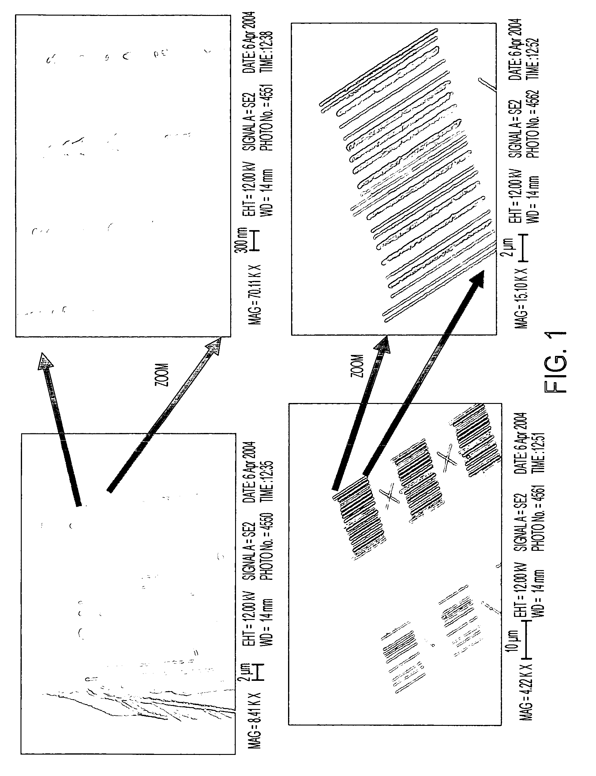
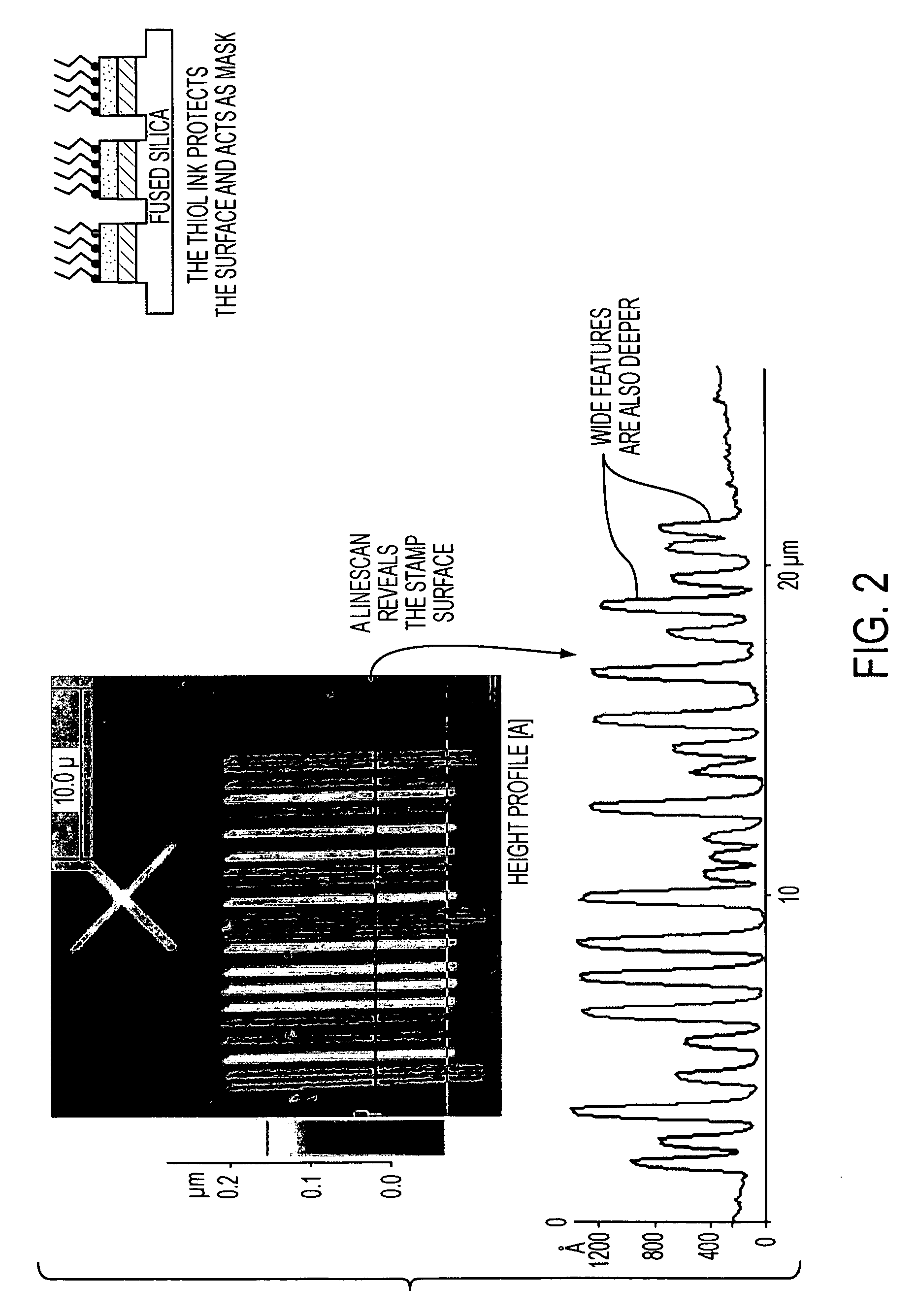
[0178]An array of 11 or 26 cantilevers (depending on the experiment) with a force constant of ˜0.05 N / m (NanoInk DPN probes style A-11 and A-26), was coated with mercaptohexadecanoic acid (MHA), more specifically by dipping them into an Acetonitrile solution containing MHA or by the following process: The cantilevers were dipped into acetonitrile with MHA, excess liquid was gently blown away using compressed air, the cantilevers were exposed to hot water steam and left in ambient conditions for drying. Then the cantilevers were again dipped in Acetonitrile containing MHA and finally excess liquid was again removed by gently blowing compressed air onto the cantilevers.

[0179]A silicon substrate was cleaned by ultrasonic actua...

embodiment 1

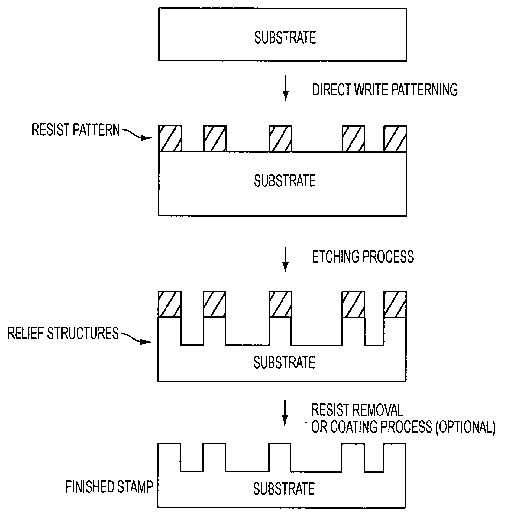
[0220]A method of preparing a template or stamp for imprinting at least one pharmaceutical composition using electron-beam direct-write nanolithography, comprising:

[0221](a) coating a substrate with a resist;

[0222](b) directing a focused electron-beam onto the resist-coated substrate to form a latent image;

[0223](c) developing the resist to form a resist pattern;

[0224](d) etching the substrate and / or depositing material onto the surface;

[0225](e) removing the resist to form a patterned substrate comprising surface topography with micron-scale or nanometer-scale lateral dimensions.

embodiment 2

[0226]A template or stamp produced by the method of Embodiment 1.


PUM

PropertyMeasurementUnit
sizeaaaaaaaaaa
sizeaaaaaaaaaa
heightaaaaaaaaaa

Abstract

Stamps and methods of making stamps for applications in anti-counterfeiting and authentication. The stamps are relatively small in size and feature nanoscale and microscale identification regions and features. High throughput manufacturing and high resolution methods are used to make the stamps including electron beam lithography and optical lithography. Anti-fouling coatings can be applied.

Description

RELATED APPLICATIONS[0001]This application claims priority to provisional application Ser. No. 60 / 637,063 filed Dec. 20, 2004 to Cruchon-Dupeyrat et al which is hereby incorporated by reference in its entirety.BACKGROUND[0002]A need exists to provide for better protection and security against counterfeiting and grey-market trading, particularly for pharmaceuticals. A review of counterfeiting in pharmaceuticals and its economic effects may be found in, for example, (1) “Counterfeit Pharmaceuticals: Current Status and Future Projections,” A. I. Wertheimer, N. M. Chaney, T. Santella, J. Am. Pharm. Assoc. 43(6):710-718, 2003, and (2) Chapter 4 of the book “Counterfeiting exposed: protecting your brand and your customers,” D. M. Hopkins, L. T. Kontnik, M. T. Turnage (Wiley, Ed. 2003); ISBN: 0471269905. Chapter 12 describes current anti-counterfeiting methods, such as holograms, intaglio printing, color-shifting technologies, and chemical or biochemical taggants. In many cases, however, m...

Claims


Application Information

Patent Timeline
Patent Type & Authority Applications(United States)
IPC IPC(8): B44B5/02
CPCG06K1/12B44B5/02
Inventor FRAGALA, JOSEPH S.LOIRET-BERNAL, CEDRICZHANG, HUASHILE, RAYMOND ROGERROSNER, BJOERNCRUCHON-DUPEYRAT, SYLVAIN
Owner NANOINK INC
Why Eureka
Try Eureka