Master slice LSI and layout method for the same

a technology of master slice and layout method, which is applied in the direction of semiconductor devices, semiconductor/solid-state device details, electrical apparatus, etc., can solve the problems of difficult to improve the integration density, the influence of miniaturization on the operation speed of the device, and the difficulty of improving the integration density

Inactive Publication Date: 2001-08-07
KK TOSHIBA
View PDF11 Cites 65 Cited by
  • Summary
  • Abstract
  • Description
  • Claims
  • Application Information

AI Technical Summary

Problems solved by technology

In these generations, harmful influences due to miniaturization have become dominant.
For example, it has become an issue that, according to miniaturization of the power supply metal wiring, generation of electromigration and / or source voltage drop of the transistors due to resistance of wiring material exert harmful influences upon an operation of the device.
In addition, since contact resistance is increased because of miniaturization of the area of the contact hole, source voltage drop of the transistors has also been caused to thus exert harmful influences upon an operation speed of the device.
In other words, it is possible that wirings other than the power supply metal wiring can be further miniaturized, but it has become difficult to improve the integration density by using the conventional wiring channel grid having uniform pitches since the line width of the power supply metal wiring, etc. determine the design rule.
As explained earlier, in the prior art wherein the pitches of the wiring channel grid are set uniformly, there is the problem that the difference between the design rule for the wiring process and the design rule for the basic cell process has become remarkable so that the integration density has not been able to enhanced.
Therefore, such problems have arisen that source voltage drop due to the wiring resistance, wiring defect caused by electromigration, etc. occur and disadvantages such as malfunction, reduction in operation speed, etc. are caused.

Method used


Image

  • Master slice LSI and layout method for the same
  • Master slice LSI and layout method for the same
  • Master slice LSI and layout method for the same

Examples


first embodiment

(First Embodiment)

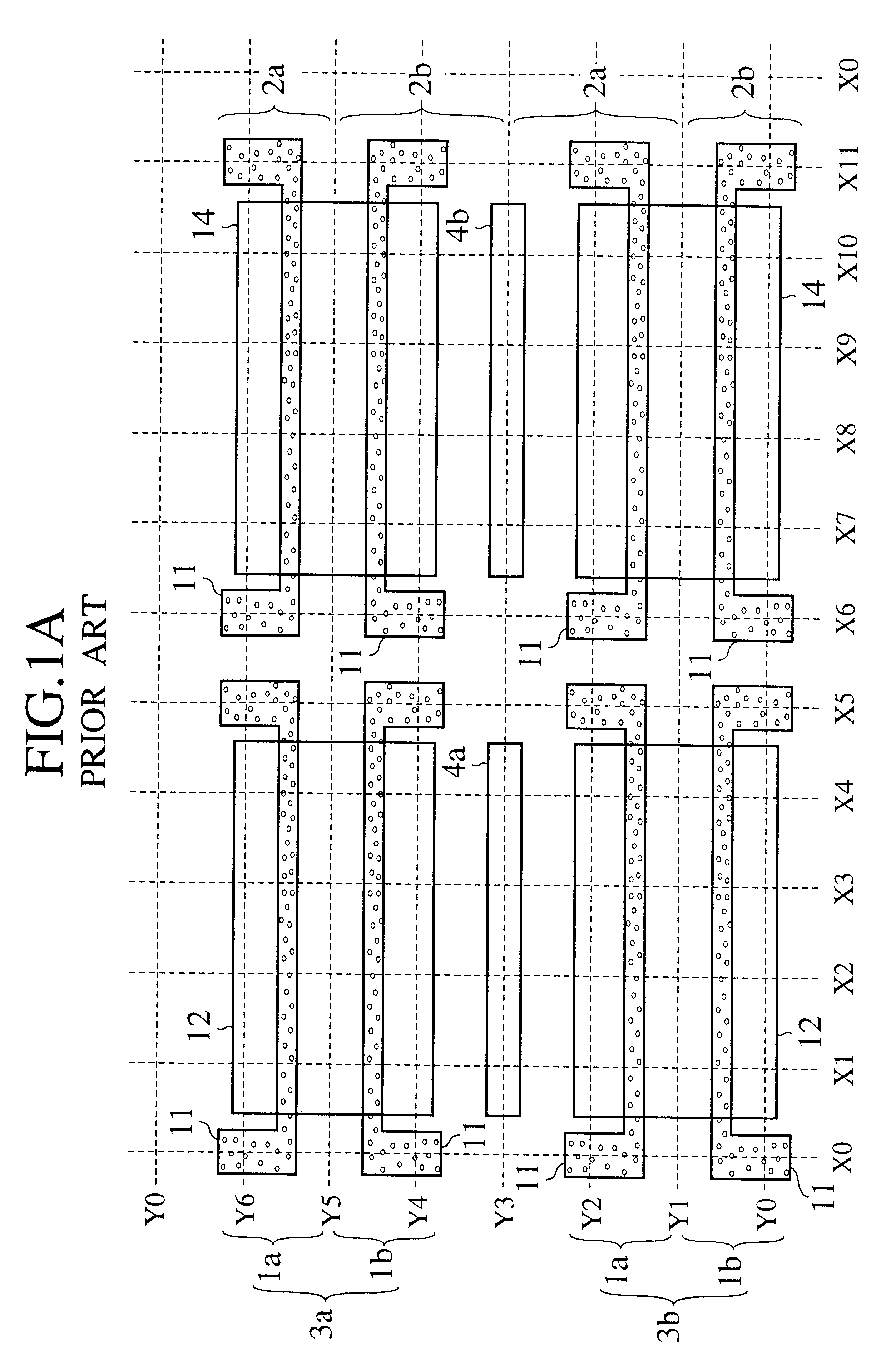
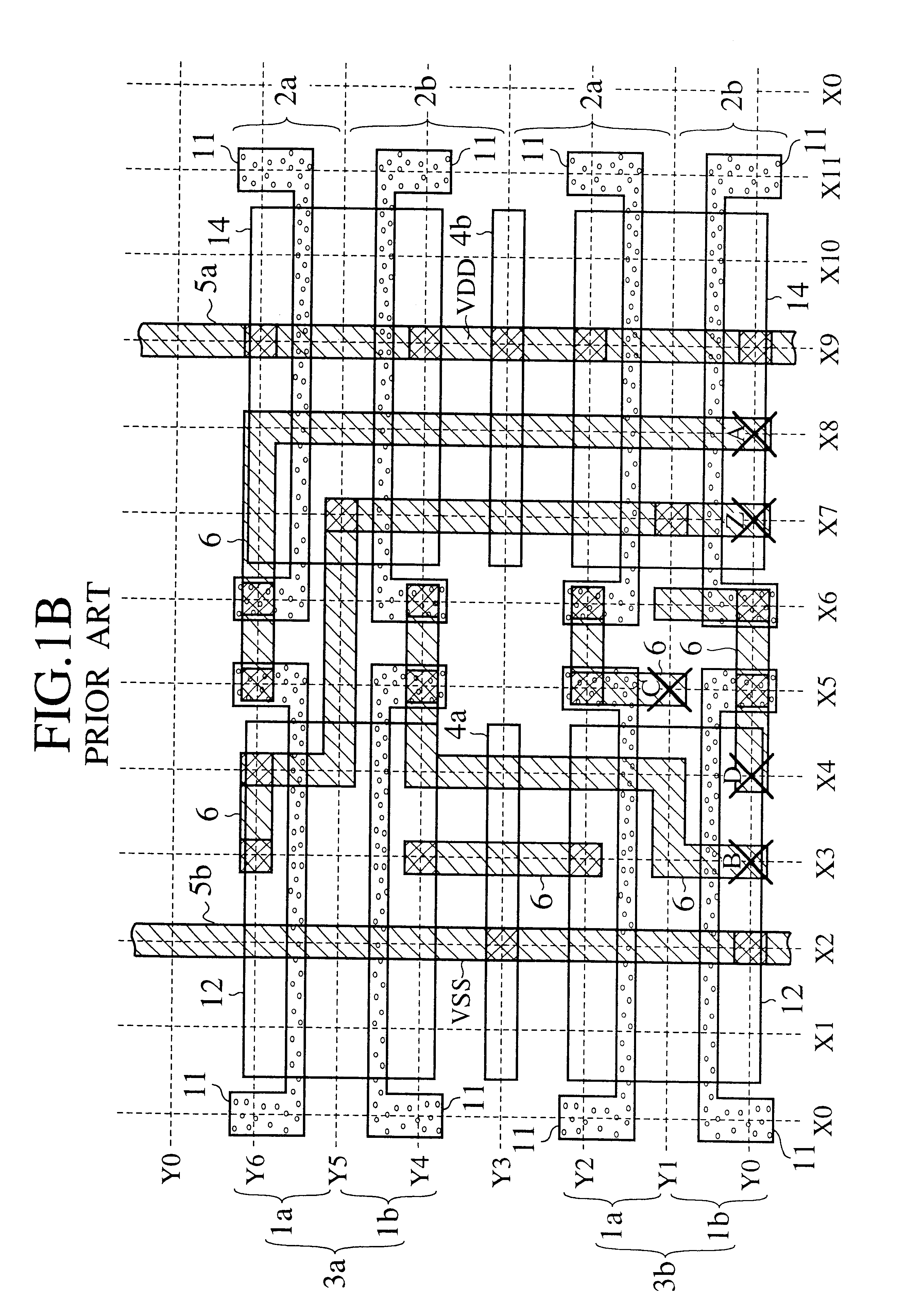
FIGS. 2A to 2D are views showing a configuration of a semiconductor integrated circuit according to a first embodiment of the present invention. FIG. 2A is a view showing layout patterns of gate basic cells, as being similar to FIG. 1A. In FIG. 2A, like references refer to like parts in FIG. 1A. A key feature of the layout shown in FIG. 2A is that, while maintaining spacings between horizontal lines Y0-Y1-Y2 and lines Y4-Y5-Y6 constituting the wiring channel grid at a predetermined (relatively wide) value, spacings of other lines in a wiring channel grid are made narrow rather than the predetermined value in order to satisfy the design rules for a spacing between a gate polysilicon region 11 and a contact hole formed on source / drain regions. This is because the scaling of the spacing between the contact hole and the polysilicon region is severe, i.e., the feature size reduction is difficult. The pitch interval which is used in the prior art may be employed as the p...

second embodiment

(Second Embodiment)

FIGS. 3A to 3C are views showing a configuration of a semiconductor integrated circuit according to a second embodiment of the present invention. A key feature of a semiconductor integrated circuit shown in FIG. 3A is that spacings between perpendicular (vertical) lines X1-X2-X3, X8-X9-X10 constituting the wiring channel grid are settled wide rather than the layout shown in FIG. 2A. In other words, in the second embodiment of the present invention, a group of horizontal (lateral) lines consist of a first set of lines Y0-Y2, Y4-Y6 having a first spacing and a second set of lines Y2-Y4, Y6-Y0 having a second spacing which being narrower than the first spacing, and a group of vertical lines consist of a third set of lines X1-X3, X8-X10 having a third spacing and a fourth set of lines X0-X1, X3-X8, X10-X11-X0 having a fourth spacing. The third spacing is made wider than the fourth spacing. Hence, as shown in FIG. 3B, a VSS (lower potential) power supply wiring 5b form...

third embodiment

(Third Embodiment)

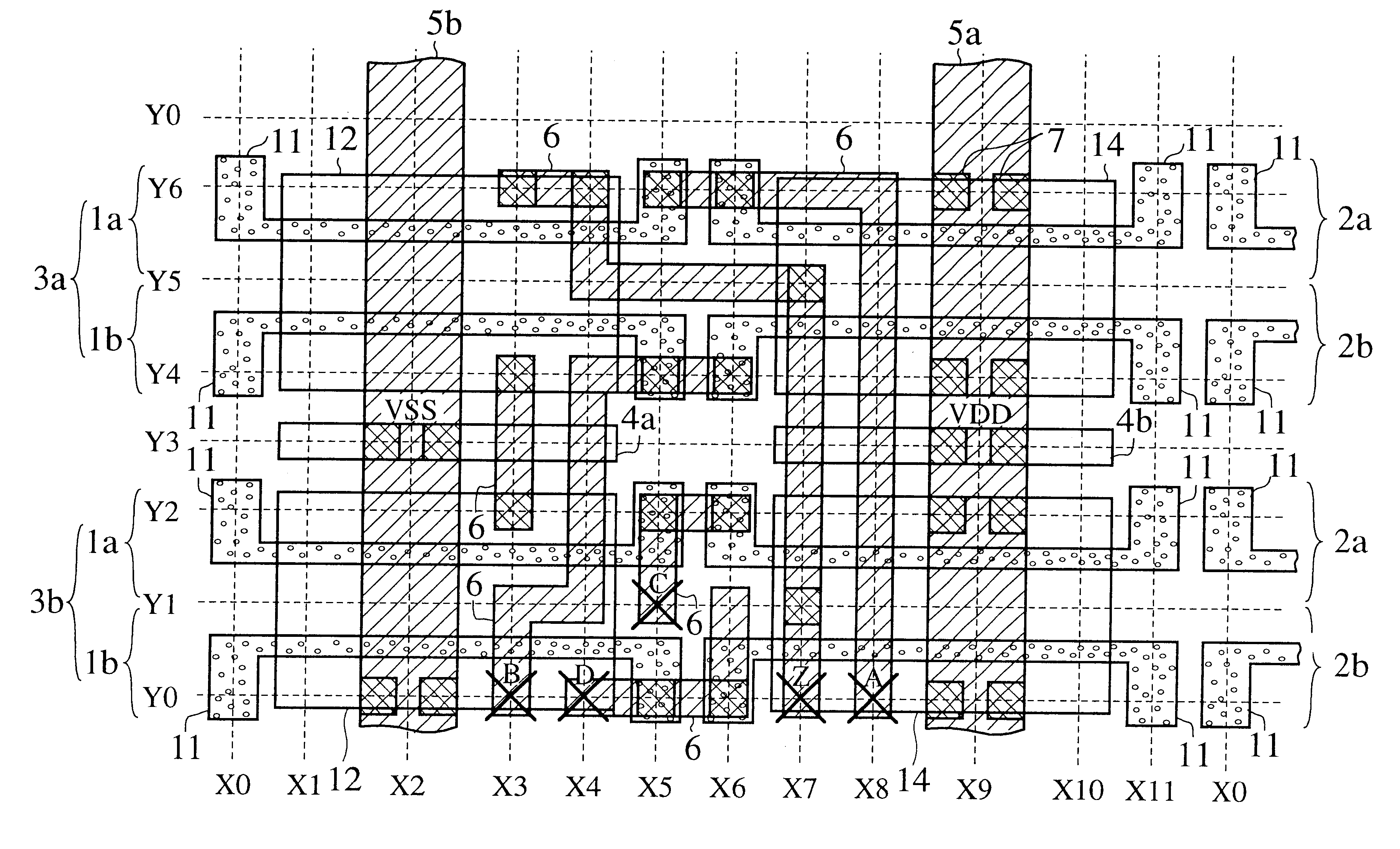
FIGS. 5A to 5C are views showing a configuration of a semiconductor integrated circuit according to a third embodiment of the present invention. A key feature of a layout of gate basic cells shown in FIG. 5A resides in the wiring channel grid comprising lateral and vertical lines, both having two kinds of spacings. Namely, lateral lines consist of the lines Y0-Y2, Y4-Y6 having the first spacing and the lines Y2-Y4, Y6-Y0 having the second spacing. And vertical lines consist of the lines X2-X3, X8-X9 having the third spacing and the lines X0-X2, X3-X8, X9-X11-X0 having the fourth spacing. In other words, in contrast to the layout shown in FIG. 2A, the third spacing between the lines X2-X3, X8-X9 is made wider than the fourth spacing between the lines X0-X2, X3-X8, X9-X11-X0. As being similar to FIG. 2A, the first spacing is set wider than the second spacing. Further, the prominent feature of the third embodiment lies in an asymmetrical disposition. Based upon the wi...


PUM


Abstract

A master slice layout technology is provided to improve integration density of a semiconductor integrated circuit such as ASIC. In particular, a plurality of gate basic cells are arranged on a semiconductor chip and then a wiring channel grid having non-uniform pitches is defined on the gate basic cells. If a layout of metal wirings is designed along the wiring channel grid, miniaturizable patterns can be set to smaller values while maintaining line widths of predetermined metal wirings such as power supply wirings at preselected values. Since flexibility for the layout of the metal wiring layers is large, miniaturization of the patterns can be attained even if design rules for basic cell process and wiring process are different.

Description

1. Field of the InventionThe present invention relates to a semiconductor device employing a master slice layout in which a plurality of gate basic cells are formed previously on an LSI chip and then only a wiring design is added to construct desired logic circuits, and to a configuration of a semiconductor device and a layout design thereof capable of improving miniaturization of wiring patterns and integration density.2. Description of the Prior ArtVarious layout designs for a semiconductor integrated circuit may be prepared according to a scale of the integrated circuit and design approach. A fully-custom IC in which all layers are designed and manufactured for exclusive use is suited for the case where a large number of high performance ICs are to be manufactured. In contrast, a semicustom IC such as Application-Specific Integrated Circuits (ASICs) in which layers located below a wiring layer level are manufactured in advance and then only wiring layers are designed and manufact...

Claims


Application Information

Patent Timeline
Patent Type & Authority Patents(United States)
IPC IPC(8): H01L27/118H01L21/3205H01L21/82H01L23/52
CPCH01L27/11803H01L2924/0002H01L2924/00
Inventor UMEMOTO, YASUNOBUUCHINO, YUKINORISEI, TOSHIKAZUMAENO, MUNEAKI
Owner KK TOSHIBA
Why Eureka
Try Eureka