Block-erase type semiconductor storage device with independent memory groups having sequential logical addresses

a semiconductor storage device and block erase technology, applied in the direction of memory address formation, memory allocation/allocation/relocation, instruments, etc., can solve the problems of data inside, inability to erase, longer time for data erase and write operations,

Inactive Publication Date: 2001-08-07
MITSUBISHI ELECTRIC CORP
View PDF9 Cites 90 Cited by
  • Summary
  • Abstract
  • Description
  • Claims
  • Application Information

AI Technical Summary

Problems solved by technology

However, while the flash memory is performing data write or data erase, data within the sector buffer cannot be erased so that the host system unit has to stop the next data transfer operation, being on standby.
This would involve longer time for data erase and write operations, as a problem.
This would involve increased cost as a problem.
That is, after the data transfer from a buffer memory to its corresponding me

Method used


Image

  • Block-erase type semiconductor storage device with independent memory groups having sequential logical addresses
  • Block-erase type semiconductor storage device with independent memory groups having sequential logical addresses
  • Block-erase type semiconductor storage device with independent memory groups having sequential logical addresses

Examples


Embodiment Construction

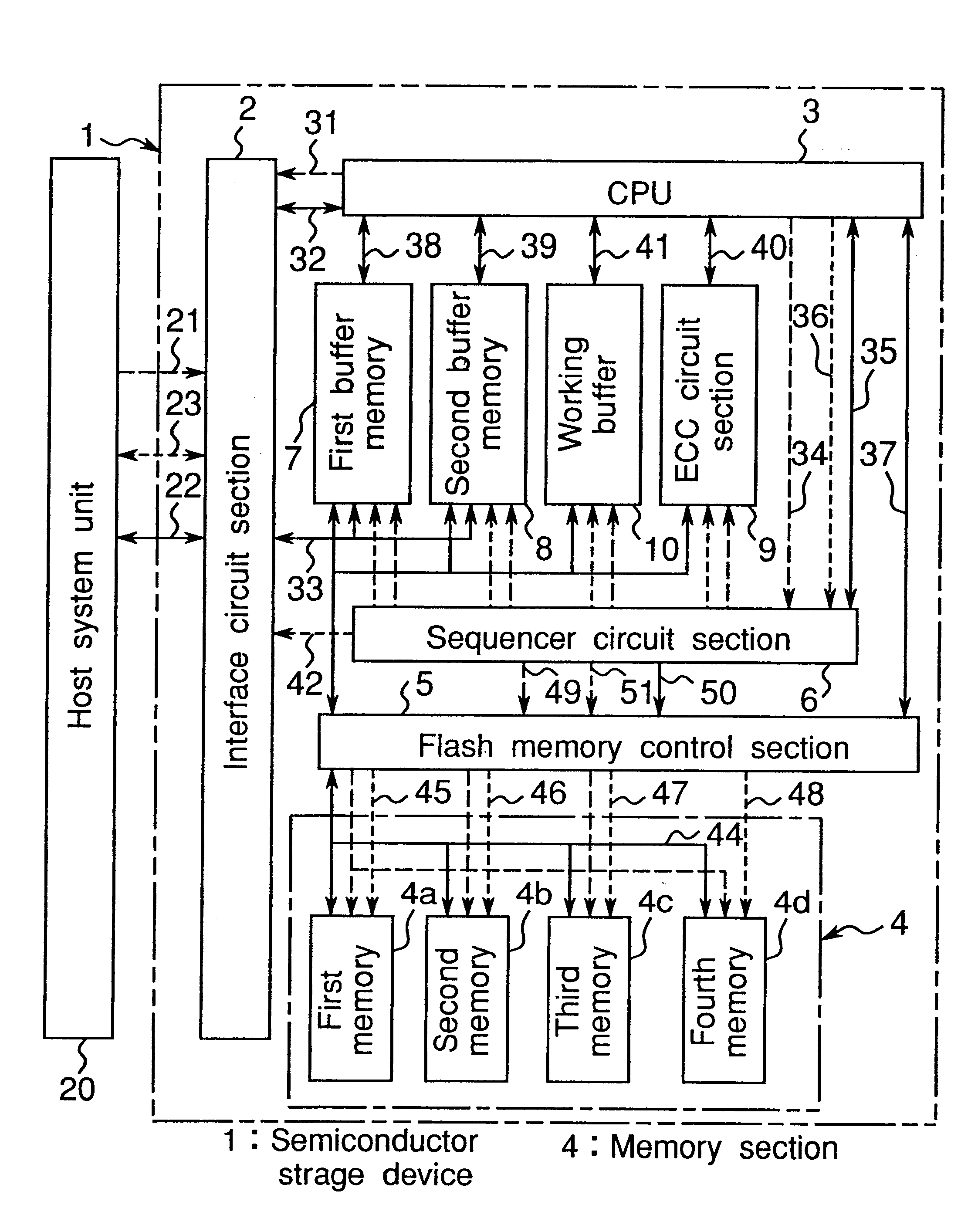
Hereinbelow, the present invention is described in detail based on an embodiment thereof as illustrated in the accompanying drawings. FIG. 1 is a schematic block diagram showing an example of the semiconductor storage device according to an embodiment of the present invention. This embodiment is explained on a case where a nonvolatile memory with a 2 Kbyte erase block unit is used. Besides, in FIG. 1, solid line represents data bus, broken line represents address bus and dotted line represents control signal line.

Referring to FIG. 1, the semiconductor storage device 1 comprises: an interface circuit section 2 for interfacing with an external host system unit 20 implemented by information processing equipment or the like; a CPU 3 for performing the control of individual circuit sections according to a command from the host system unit 20; a memory section 4 comprising a plurality of IC memories implemented by block-erase type flash memory; a flash memory control section 5 for perform...


PUM


Abstract

A semiconductor storage device having a plurality of block-erase type non volatile memory chips classifies the memory chips into memory groups of a number equal to twice the number of buffer memories provided in the storage device and assigns logic sector addresses sequentially to sectors contained in one erase block of each memory group in such a manner that the logic sector addresses are sequenced in series to those in the corresponding erase block of the next succeeding memory group.

Description

1. Field of the InventionThe present invention relates to a semiconductor storage device using nonvolatile memory as a storage medium and, more particularly, to a semiconductor storage device using nonvolatile memory such as block-erase type flash memory.2. Description of the Prior ArtIn a semiconductor storage device using block-erase type nonvolatile memory, for example, flash memory, the flash memory can write or read data only in steps of 8 bits or 16 bits. In contrast to this, a host system unit comprising information processing equipment or the like that makes access to the semiconductor storage device performs data transfer in steps of, for example, 512 B. Therefore, the semiconductor storage device is equipped with one sector buffer as buffer memory for temporarily storing data.However, while the flash memory is performing data write or data erase, data within the sector buffer cannot be erased so that the host system unit has to stop the next data transfer operation, being ...

Claims


Application Information

Patent Timeline
IPC IPC(8): G06F12/02G06F3/06G11C11/34G06F12/00G06F12/06G11C16/02
CPCG06F3/0613G06F3/064G06F3/0679G06F12/0246G06F3/0652G06F2212/7208
Inventor MIYAUCHI, SHIGENORI
Owner MITSUBISHI ELECTRIC CORP
Why Eureka
Try Eureka