Semiconductor device
a technology of semiconductors and devices, applied in the direction of semiconductor devices, electrical apparatus, transistors, etc., can solve the problem of low reliability and achieve the effects of high productivity, miniaturization or high integration, and favorable electrical characteristics
- Summary
- Abstract
- Description
- Claims
- Application Information
AI Technical Summary
Benefits of technology
Problems solved by technology
Method used
Image

Examples
embodiment 1
1>
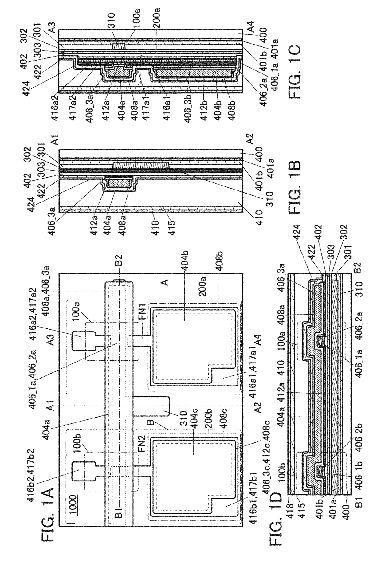
[0075]FIG. 8 is a circuit diagram illustrating part of a memory cell array included in a semiconductor device 1000. FIG. 8 illustrates a circuit diagram of two memory cells, a memory cell A and a memory cell B, and the memory cell A is a memory cell at a right end of the memory cell array. The memory cell included in the semiconductor device 1000 are repeatedly provided in the upper, lower, and left directions (denoted by dotted lines in FIG. 8).
[0076]The memory cell A includes a transistor 100a including a first gate electrode and a second gate electrode, a transistor 600a, a capacitor 200a, and a node FN1. Furthermore, the memory cell B includes a transistor 100b including a first gate electrode and a second gate electrode, a transistor 600b, a capacitor 200b, and a node FN2. The connection region of one of a source electrode and a drain electrode of the transistor 100a and one electrode of the capacitor 200a can be referred to as the node FN1. Furthermore, the connection region...
embodiment 2
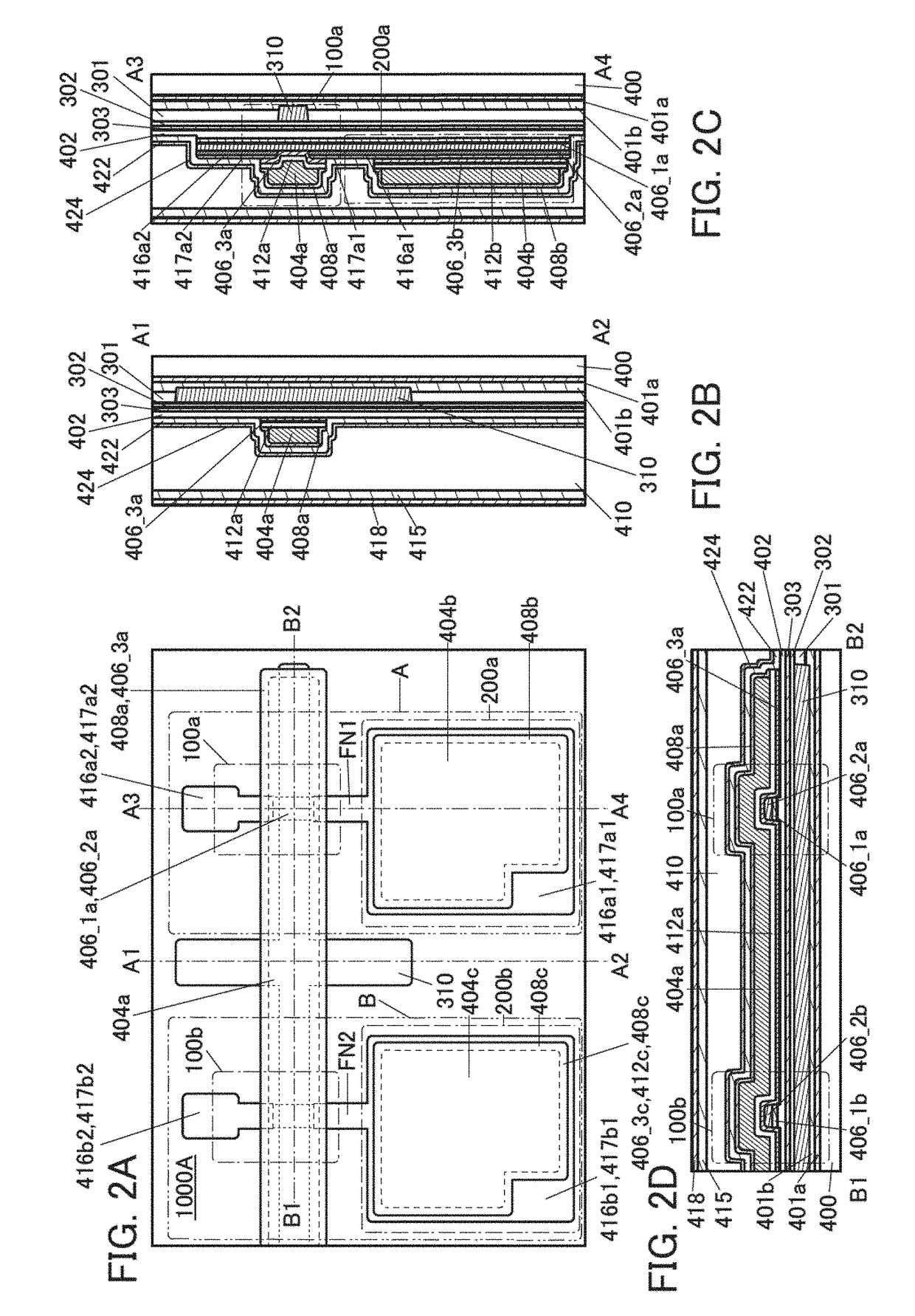
[0190]A method for manufacturing the semiconductor device 1000 of one embodiment illustrated in FIGS. 1A to 1D will be described below with reference to FIGS. 9A to 9D to FIGS. 18A to 18D. FIGS. 9A to 18A are top views. FIGS. 9B to 18B are cross-sectional views taken along dashed-dotted line A1-A2 in FIGS. 9A to 18A. FIGS. 9C to 18C are cross-sectional views taken along dashed-dotted line A3-A4 in FIGS. 9A to 18A. FIGS. 9D to 18D are cross-sectional views taken along dashed-dotted line B1-B2 in FIGS. 9A to 18A.
[0191]First, the substrate 400 is prepared.
[0192]Next, the insulator 401a is formed. The insulator 401a can be formed by a sputtering method, a chemical vapor deposition (CVD) method, a molecular beam epitaxy (MBE) method, a pulsed laser deposition (PLD) method, an atomic layer deposition (ALD) method, or the like.
[0193]CVD methods can be classified into a plasma enhanced CVD (PECVD) method using plasma, a thermal CVD (TCVD) method using heat, a photo CVD method using light, a...
embodiment 3
[0245]In this embodiment, an example of a semiconductor device including any of the transistors disclosed in this specification and the like is described.
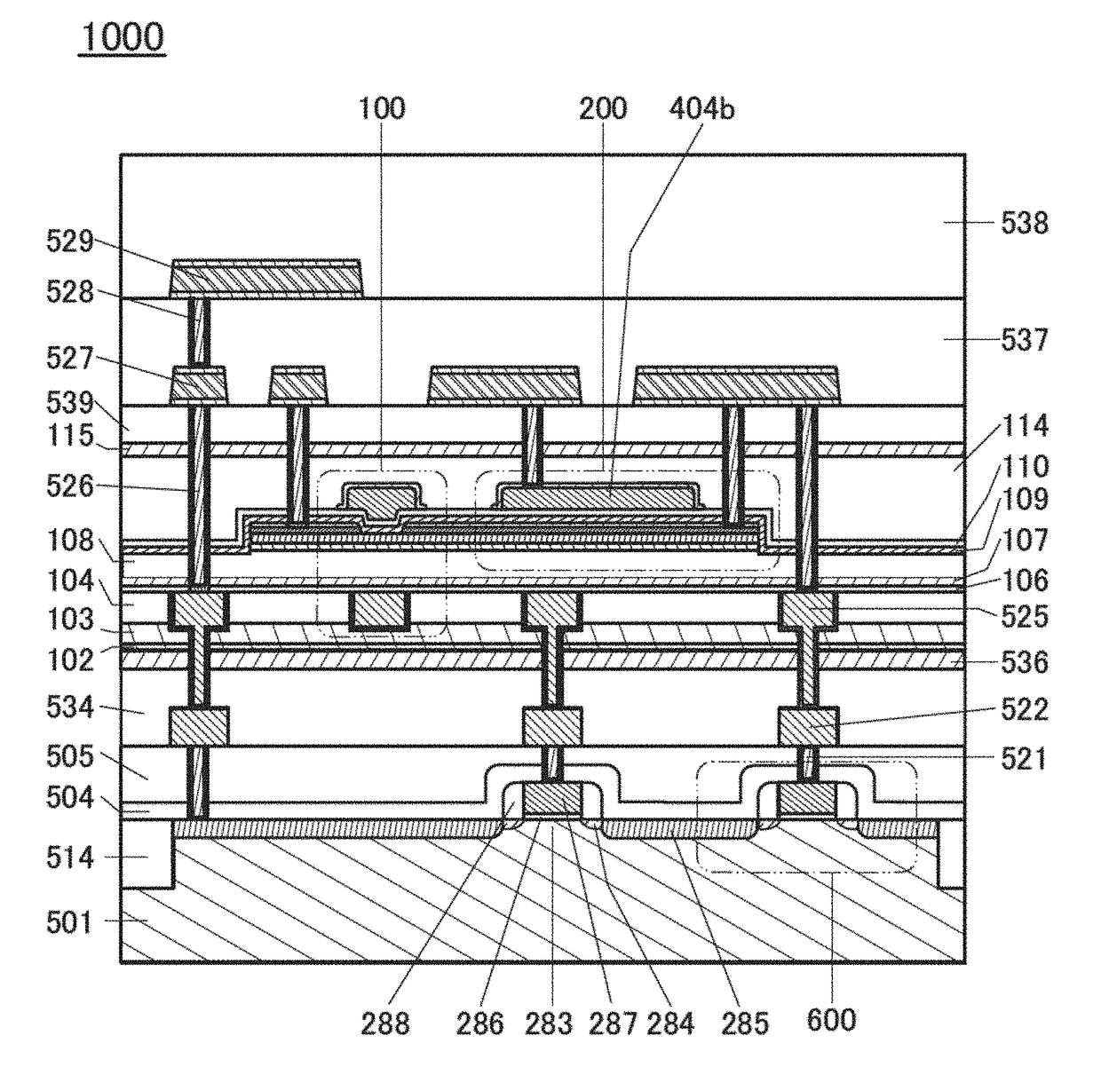
[0246]FIG. 19 is a cross-sectional view of a semiconductor device 1000. The semiconductor device 1000 includes the transistor 100, the transistor 600, and a capacitor 200. The transistors 100 and 600 and the capacitor 200 correspond to the transistors 100a and 600a and the capacitor 200a illustrated in FIG. 8, respectively.
[0247]In the semiconductor device 1000, an n-type semiconductor is used for a substrate 501. The transistor 600 includes a channel formation region 283, high-concentration p-type impurity regions 285, an insulator 286, a conductor 287, and a sidewall 288. In regions overlapping with the sidewall 288 with the insulator 286 located therebetween, low-concentration p-type impurity regions 284 are provided. The insulator 286 can function as a gate insulator. The conductor 287 can function as a gate conductor. The chan...
PUM
 Abstract
Description
Claims
Application Information
 - R&D
- Intellectual Property
- Life Sciences
- Materials
- Tech Scout
- Unparalleled Data Quality
- Higher Quality Content
- 60% Fewer Hallucinations
Browse by: Latest US Patents, China's latest patents, Technical Efficacy Thesaurus, Application Domain, Technology Topic, Popular Technical Reports.
© 2025 PatSnap. All rights reserved.Legal|Privacy policy|Modern Slavery Act Transparency Statement|Sitemap|About US| Contact US: help@patsnap.com