Transistor

a technology of transistors and transistors, applied in the direction of transistors, semiconductor devices, electrical apparatus, etc., can solve the problems of low reliability, and achieve the effects of high productivity, miniaturization or high integration, and good electrical characteristics

Inactive Publication Date: 2017-12-28
SEMICON ENERGY LAB CO LTD
View PDF10 Cites 2 Cited by
  • Summary
  • Abstract
  • Description
  • Claims
  • Application Information

AI Technical Summary

Benefits of technology

[0011]An object of one embodiment of the present invention is to provide a semiconductor device having good electrical characteristics. Another object of one embodiment of the present invention is to provide a semiconductor device that can be miniaturized or highly integrated. Another object of one embodiment of the present invention is to provide a semiconductor device that can be manufactured with high productivity.
[0012]Another object of one embodiment of the present invention is to provide a semiconductor device capable of retaining data for a long time. Another object of one embodiment of the present invention is to provide a semiconductor device capable of high-speed data writing. Another object of one embodiment of the present invention is to provide a semiconductor device with high design flexibility. Another object of one embodiment of the present invention is to provide a low-power semiconductor device. Another object of one embodiment of the present invention is to provide a novel semiconductor device.
[0033]One embodiment of the present invention can provide a semiconductor device having good electrical characteristics. Another embodiment of the present invention can provide a semiconductor device that can be miniaturized or highly integrated. Another embodiment of the present invention can provide a semiconductor device that can be manufactured with high productivity.
[0034]Another embodiment of the present invention can provide a semiconductor device capable of retaining data for a long time. Another embodiment of the present invention can provide a semiconductor device capable of high-speed data writing. Another embodiment of the present invention can provide a semiconductor device with high design flexibility. Another embodiment of the present invention can provide a low-power semiconductor device. Another embodiment of the present invention can provide a novel semiconductor device.

Problems solved by technology

However, it is known that a transistor including an oxide semiconductor in a channel region has a problem in that the electrical characteristics are likely to be changed by impurities and oxygen vacancies in the oxide semiconductor and thus the reliability is low.

Method used


Image

  • Transistor
  • Transistor
  • Transistor

Examples


embodiment 1

1>

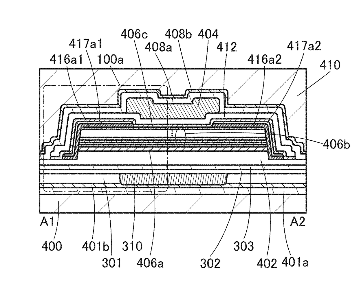
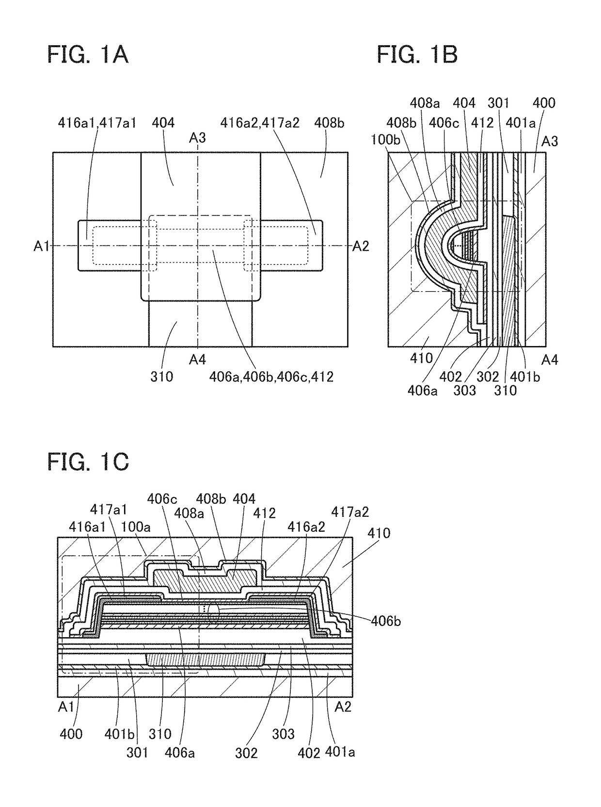
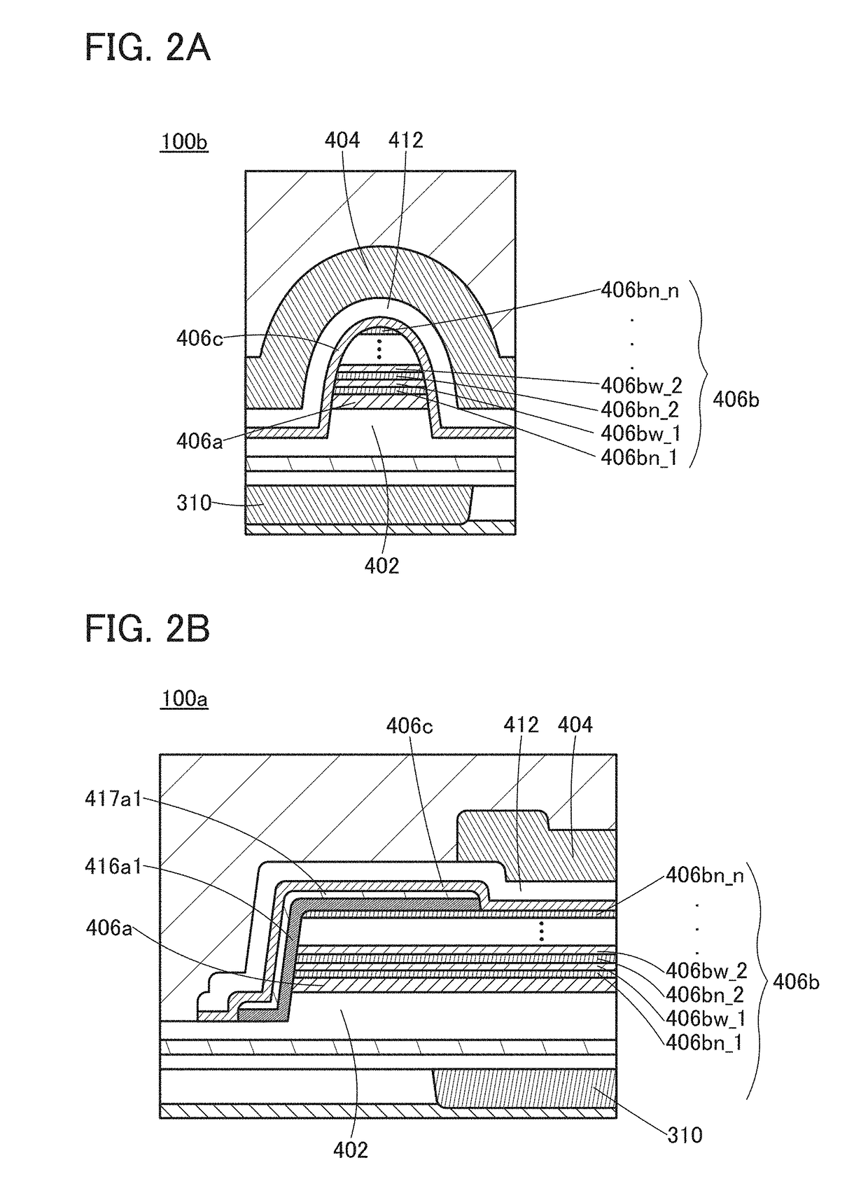
[0086]FIG. 1A is a top view of a transistor of one embodiment of the present invention. FIG. 1B is a cross-sectional view taken along the dashed-dotted line A3-A4 in FIG. 1A. That is, FIG. 1B is a cross-sectional view in the channel width direction of a channel formation region of the transistor. FIG. 1C is a cross-sectional view taken along the dashed-dotted line A1-A2 in FIG. 1A. That is, FIG. 1C is a cross-sectional view in the channel length direction of the transistor. Some components are not illustrated in the top view in FIG. 1A for simplification of the drawing.

[0087]In FIGS. 1B and 1C, the transistor is provided over an insulator 401b over a substrate 400. The insulator 401b is provided over the substrate 400 with an insulator 401a therebetween. The transistor includes: an insulator 301; a conductor 310 in an opening provided in the insulator 301; an insulator 302 over the conductor 310 and the insulator 301; an insulator 303 over the insulator 302; an insulator 402 over ...

embodiment 2

[0247]A method for manufacturing the transistor of one embodiment of the present invention illustrated in FIGS. 1A to 1C will be described below with reference to FIGS. 1A to 1C, FIGS. 11A to 11C, FIGS. 12A to 12C, FIGS. 13A to 13C, and FIGS. 14A to 14C. FIG. 1A, FIG. 11A, FIG. 12A, FIG. 13A, and FIG. 14A are top views. FIG. 1B, FIG. 11B, FIG. 12B, FIG. 13B, and FIG. 14B are cross-sectional views taken along the dashed-dotted line A3-A4 in FIG. 1A, FIG. 11A, FIG. 12A, FIG. 13A, and FIG. 14A, respectively. FIG. 1C, FIG. 11C, FIG. 12C, FIG. 13C, and FIG. 14C are cross-sectional views taken along the dashed-dotted line A1-A2 in FIG. 1A, FIG. 11A, FIG. 12A, FIG. 13A, and FIG. 14A, respectively.

[0248]First, the substrate 400 is prepared.

[0249]Then, the insulator 401a is deposited. The insulator 401a can be deposited by a sputtering method, a chemical vapor deposition (CVD) method, a molecular beam epitaxy (MBE) method, a pulsed laser deposition (PLD) method, an atomic layer deposition (A...

embodiment 3

[0301]In this embodiment, embodiments of semiconductor devices will be described with reference to FIGS. 19 and 20.

[Memory Device]

[0302]FIGS. 19 and 20 each illustrate an example of a memory device in which the semiconductor device of one embodiment of the present invention is used.

[0303]The memory devices in FIGS. 19 and 20 each include a transistor 900, a transistor 800, a transistor 700, and a capacitor 600.

[0304]The transistor 700 is similar to the transistor described in the above embodiment with reference to FIGS. 1A to 1C or the like. An insulator 712 illustrated in FIGS. 19 and 20 corresponds to the insulator 401a. An insulator 714 corresponds to the insulator 401b. An insulator 716 corresponds to the insulator 301. An insulator 720 corresponds to the insulator 302. An insulator 722 corresponds to the insulator 303. An insulator 724 corresponds to the insulator 402. An insulator 772 corresponds to the insulator 408a. An insulator 774 corresponds to the insulator 408b. An ins...


PUM


Abstract

A gate insulator is between a gate electrode and a metal oxide. The gate electrode includes a region overlapping with the metal oxide with the gate insulator therebetween. First and second conductors each include a region in contact with the top and side surfaces of the metal oxide. The metal oxide has a layered structure in which oxides each having a first band gap and oxides each having a second band gap and being adjacent to the oxide having the first band gap are alternately stacked in a thickness direction. The number of oxides each having the first band gap in the metal oxide is two or more. The first band gap is smaller than the second band gap by 0.3 eV to 1.3 eV inclusive. The oxide having the first band gap is In oxide or In—Zn oxide. The oxide having the second band gap is In-M-Zn oxide.

Description

BACKGROUND OF THE INVENTION1. Field of the Invention[0001]Embodiments of the present invention relate to a transistor, a semiconductor device, and a method for driving the semiconductor device. Another embodiment of the present invention relates to an electronic device.[0002]Note that one embodiment of the present invention is not limited to the above technical field. One embodiment of the invention disclosed in this specification and the like relates to an object, a method, or a manufacturing method. One embodiment of the present invention relates to a process, a machine, manufacture, or a composition of matter.[0003]In this specification and the like, a semiconductor device refers to every device that can function by utilizing semiconductor characteristics. A display device (e.g., a liquid crystal display device and a light-emitting display device), a projection device, a lighting device, an electro-optical device, a power storage device, a memory device, a semiconductor circuit, ...

Claims


Application Information

Patent Timeline
Patent Type & Authority Applications(United States)
IPC IPC(8): H01L29/786H01L29/24
CPCH01L29/24H01L29/7869H01L29/41733H01L29/78648H01L29/78696H01L27/1225
Inventor YAMAZAKI, SHUNPEI
Owner SEMICON ENERGY LAB CO LTD
Why Eureka
Try Eureka