Integrated circuit capacitor

a technology of integrated circuit capacitors and capacitors, which is applied in the direction of capacitors, semiconductor devices, electrical apparatus, etc., can solve the problems of difficult processing of materials compatible with hdc dielectrics, difficult device manufacture, and difficult material processing of materials which are difficult to manufactur

Inactive Publication Date: 2001-09-25
TEXAS INSTR INC
View PDF10 Cites 383 Cited by
  • Summary
  • Abstract
  • Description
  • Claims
  • Application Information

AI Technical Summary

Problems solved by technology

This approach becomes very difficult in terms of manufacturability for devices such as the 256 Mbit and 1 Gbit DRAMs.
Unfortunately, the materials which are compatible with HDC dielectrics tend to be difficult to process.
Accordingly, techniques to deposit and etch materials other than those commonly used are not well known.
As a result, it is presently difficult to use HDC materials in anything but the simplest structures.

Method used


Image

  • Integrated circuit capacitor
  • Integrated circuit capacitor
  • Integrated circuit capacitor

Examples


Embodiment Construction

The making and use of the various embodiments are discussed below in detail. However, it should be appreciated that the present invention provides many applicable inventive concepts which can be embodied in a wide variety of specific contexts. The specific embodiments discussed are merely illustrative of specific ways to make and use the invention, and do not limit the scope of the invention.

The structure of the present invention will be described first. A method of fabricating a simple structure will then be described. Finally, the present invention will be described in terms of one specific application--the dynamic random access memory.

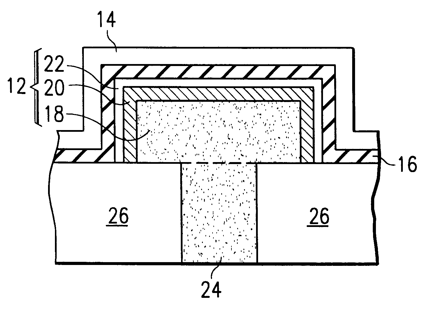
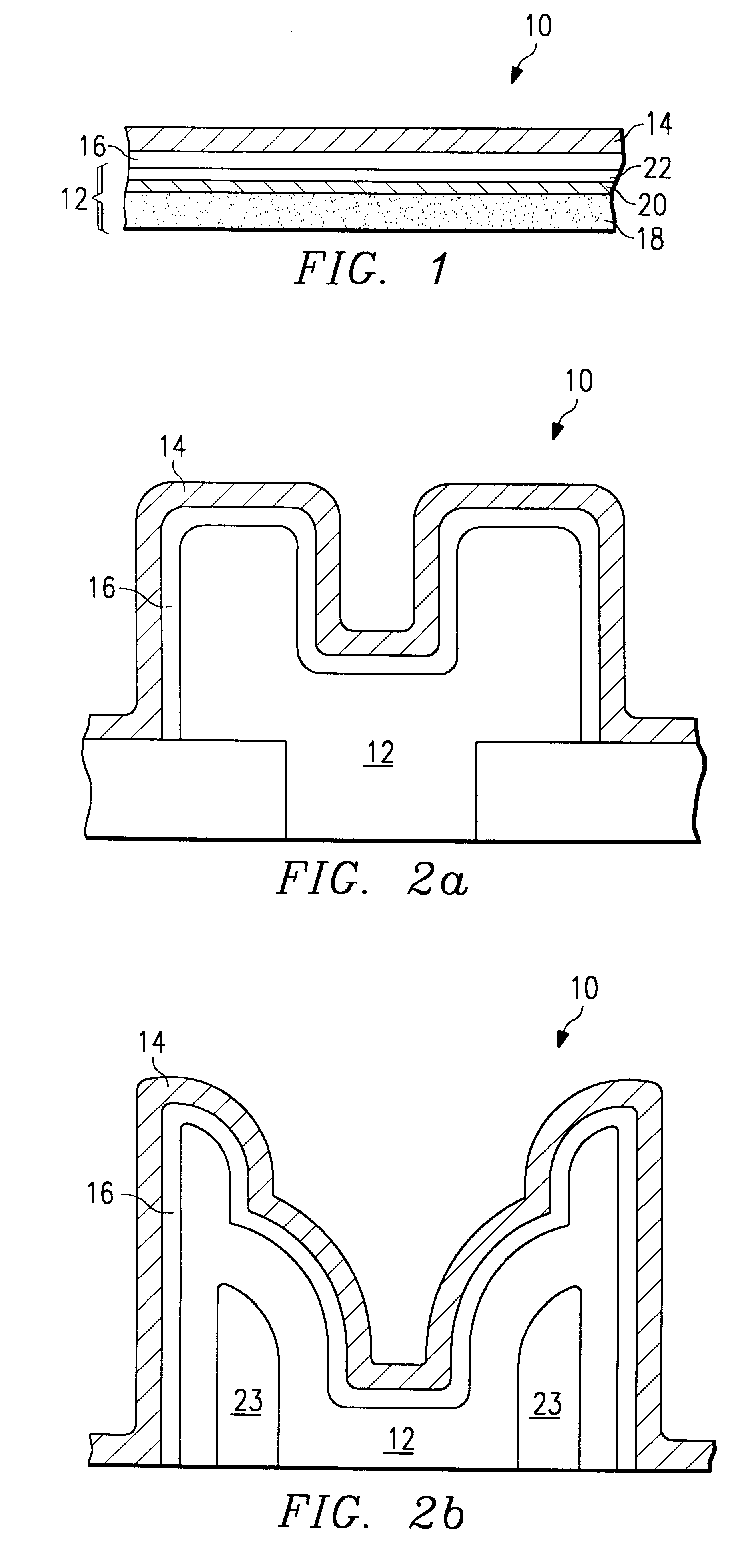
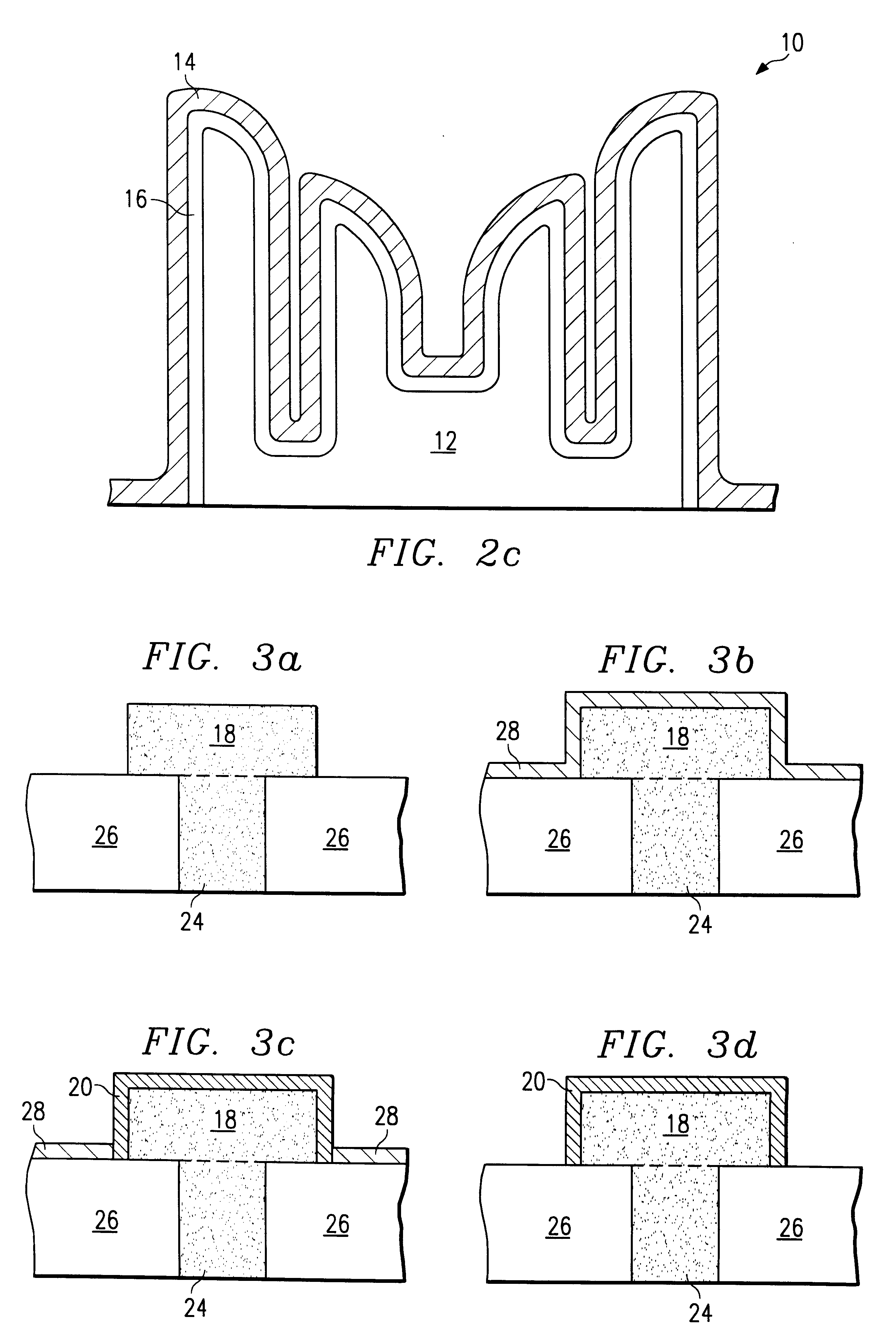
FIG. 1 illustrates a simplified view of a first embodiment integrated circuit capacitor 10 of the present invention. It is noted in viewing FIG. 1, as well as subsequent figures, that no attempt has been made to draw the various levels to scale. Specific dimensions will be provided in the written description when warranted.

Capacitor 10 includes a fi...


PUM


Abstract

The present invention discloses a novel integrated circuit capacitor and a method of forming such a capacitor. The capacitor formation begins with a base electrode 18 adjacent an insulating region 26. This base electrode 18 can comprise either polysilicon or a metal. A layer 28 of a first material, such as a siliciding metal, is formed over the base electrode 18 as well as the adjacent insulating region. A self-aligned capacitor electrode 12 can then be formed by reacting the first material 28 with the base electrode 18 and removing unreacted portions of the first material 28 from the insulating region 26. The capacitor is then completed by forming a dielectric layer 16 over the self-aligned capacitor electrode 12 and a second capacitor electrode 14 over the dielectric layer 16.

Description

RELATED PATENT APPLICATIONThis invention is related to concurrently filed applications Ser. No. 09 / 014484 (TI-21973) and Ser. No. (TI-23343) which are each incorporated herein by reference.1. Field of the InventionThis invention relates generally to semiconductor devices and specifically to an integrated circuit capacitor and a method of forming a capacitor.2. BACKGROUND OF THE INVENTIONThe increasing density of integrated circuits (e.g., dynamic random access memories) is increasing the need for materials with high dielectric constants to be used in electrical devices such as capacitors. Generally, capacitance is directly related to the surface area of the electrode in contact with the capacitor dielectric, but is not significantly affected by the electrode volume. The current method generally utilized to achieve higher capacitance per unit area is to increase the surface area / unit area by increasing the topography, such as in trench and stack capacitors using SiO.sub.2 or SiO.sub....

Claims


Application Information

Patent Timeline
Patent Type & Authority Patents(United States)
IPC IPC(8): H01L21/02H01L21/60H01L21/285H01L27/108H01L21/8242
CPCH01L28/75H01L28/55H01L21/28518H01L21/76897H01L28/90H01L27/10
Inventor TSU, ROBERTASANO, ISAMUIIJIMA, SHINPEIMCKEE, WILLIAM R.
Owner TEXAS INSTR INC
Why Eureka
Try Eureka