Data strobe buffer in SDRAM

a data strobe and buffer technology, applied in the field of data strobe buffer in sdram, can solve the problems of high chip rate, unusable output generation, and misoperation of the chip

Inactive Publication Date: 2001-11-06
HYUNDAI ELECTRONICS IND CO LTD
View PDF6 Cites 18 Cited by
  • Summary
  • Abstract
  • Description
  • Claims
  • Application Information

AI Technical Summary

Problems solved by technology

Accordingly, even if a small fluctuation of the DS signal occurs, an undesirable output is generated.
The undesirable output of the data strobe buffer makes the chip rate higher.
Also, th

Method used


Image

  • Data strobe buffer in SDRAM
  • Data strobe buffer in SDRAM
  • Data strobe buffer in SDRAM

Examples


Embodiment Construction

Hereinafter, preferred embodiments of the present invention will be described in detail with reference to the accompanying drawings.

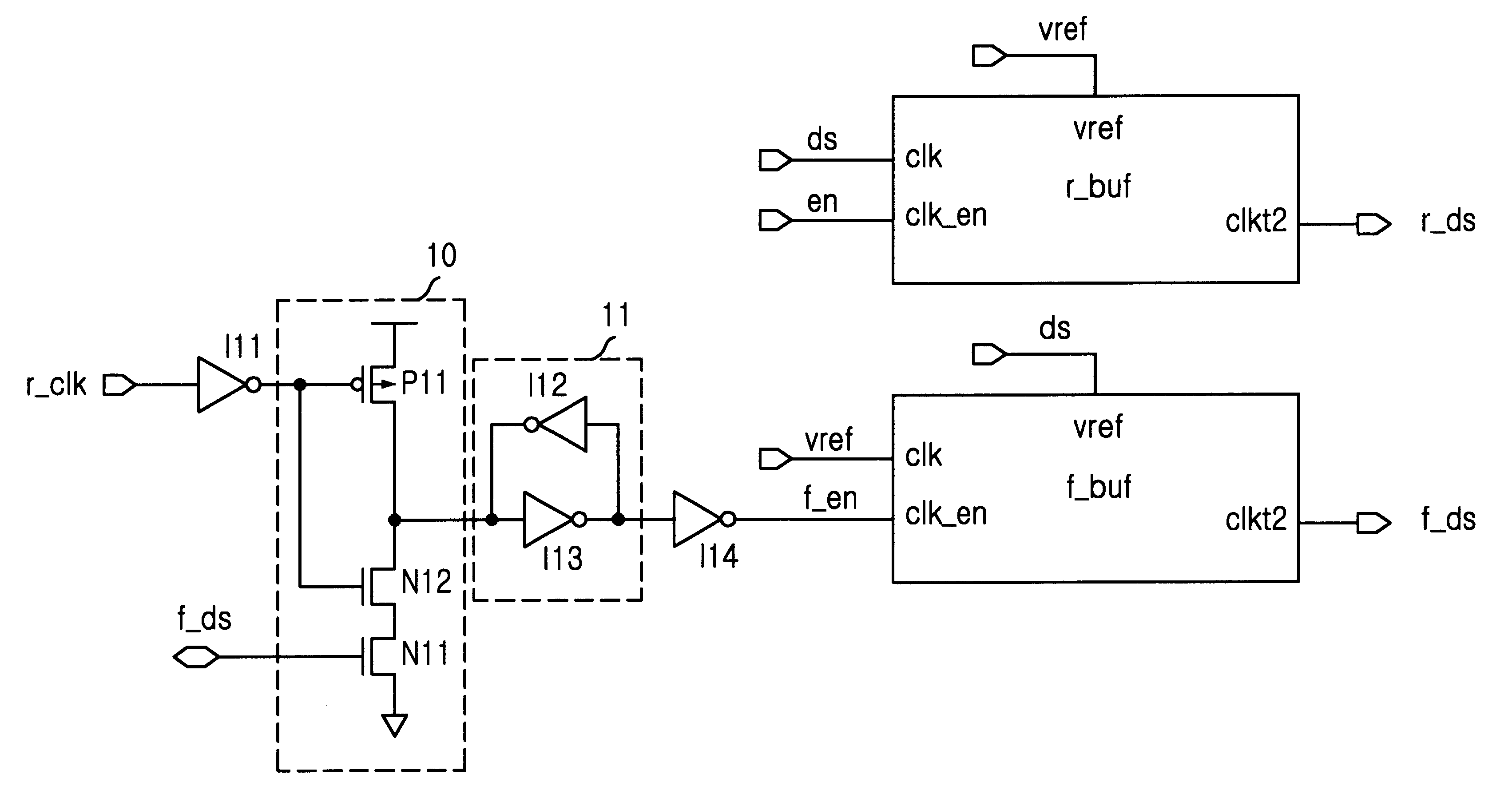
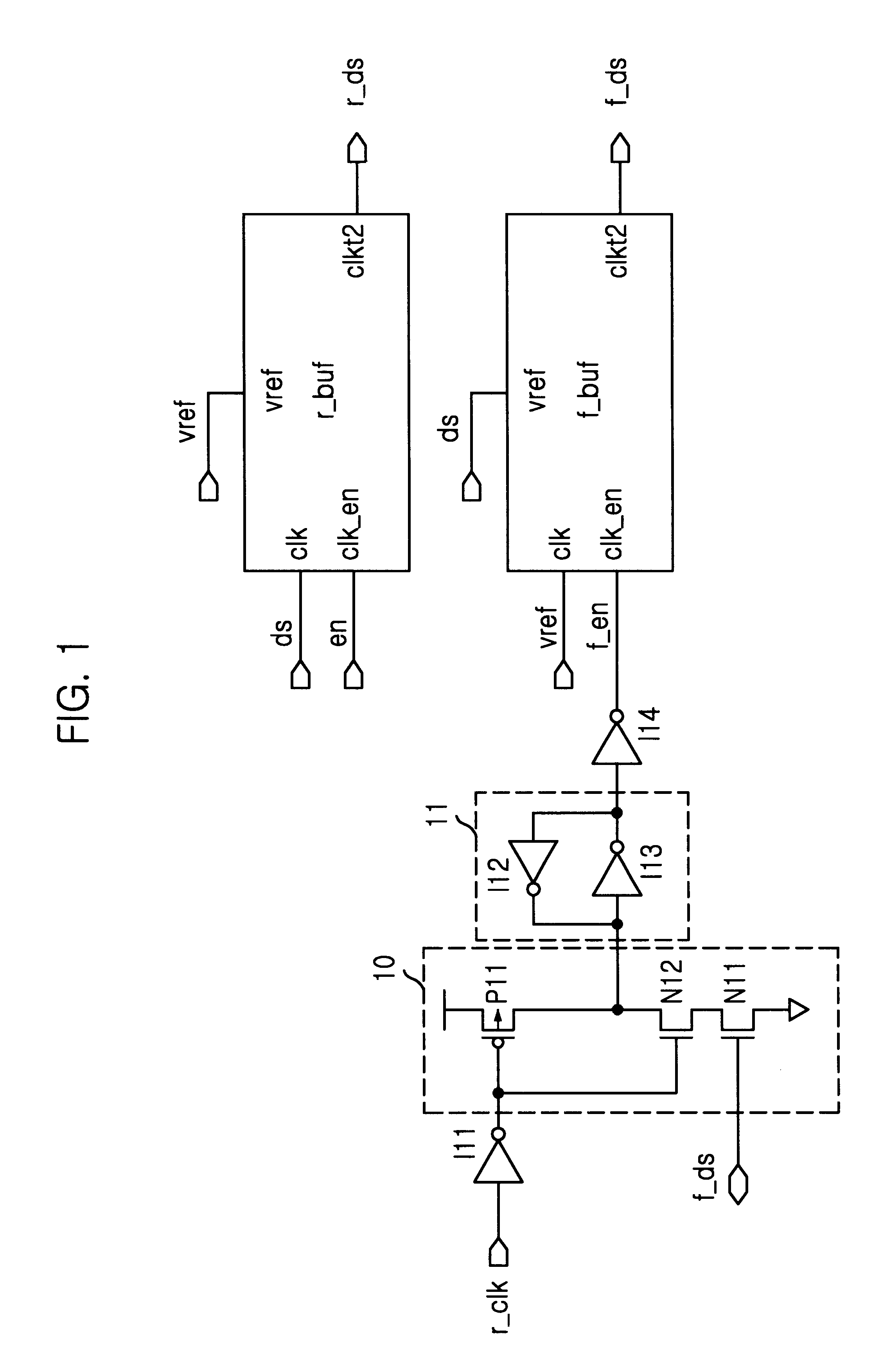
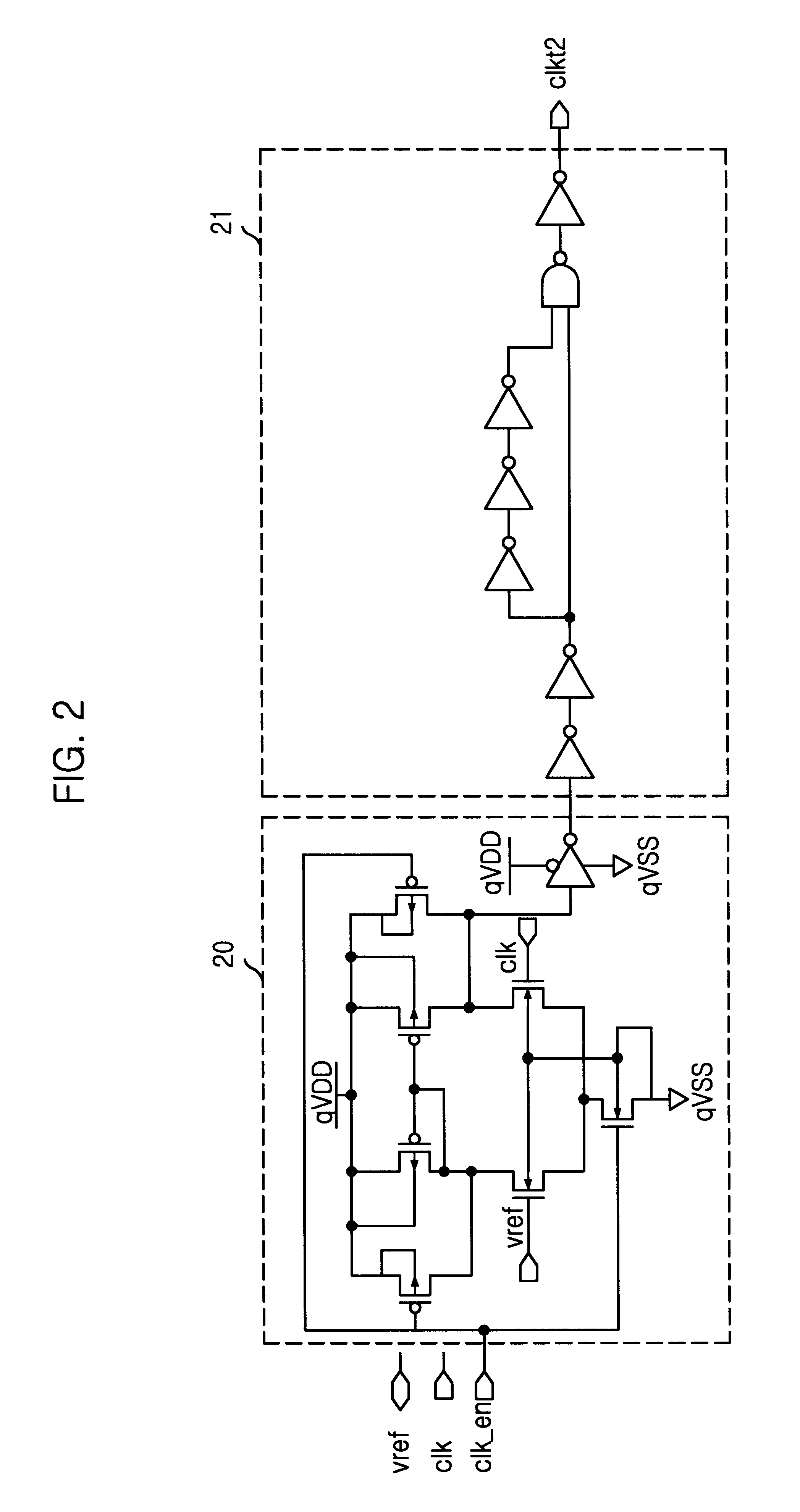
FIG. 1 is a circuit diagram of a data strobe buffer in accordance with one embodiment of the present invention.

A data strobe buffer (hereinafter, as is referred to "DS buffer") includes two dynamic buffers. A first dynamic buffer r_buf generates a pulse on a rising edge of a data strobe signal ds. A second dynamic buffer f_buf generates a pulse on a falling edge of the data strobe signal ds.

The first dynamic buffer r_buf receives a reference voltage vref having the same level as a high impedance state through a first input end vref, a data strobe signal ds (hereinafter, as is referred to "DS signal") through a second input end clk and a first buffer enable signal en through a third input end clk_en. The first dynamic buffer r_buf generates a first pulse r_ds which goes to a logic high state at the rising edge of the DS signal ds, and outputs the first p...


PUM


Abstract

A data strobe buffer in SDRAM is disclosed. The data strobe buffer for a synchronous dynamic read only memory (SDRAM), comprising: a first dynamic buffer generating a first pulse at a rising edge of a data strobe signal; a second dynamic buffer generating a second pulse at a falling edge of the data strobe signal; and a block for generating an enable signal which is enabled in a range between a rising edge of an external clock signal and a logic high state of the second pulse, and providing the second dynamic buffer with the enable signal. The data strobe buffer ensures a minimum value of tDQSS parameter in DDR SDRAM even if speed of the chip increases or operation condition of the chip becomes tight, thereby preventing the data strobe buffer from being misoperated due to the damping and the fluctuation of the data strobe signal.

Description

The present invention relates to a memory device; and, more particularly, to a data strobe buffer applicable to a synchronous dynamic random access memory (SDRAM).DESCRIPTION OF THE PRIOR ARTFor achieving a high speed operation in a dynamic random access memory (DRAM), synchronous DRAMs (hereinafter, as is referred to "SDRAMs") have been developed. The SDRAM operates in synchronization with an external clock signal. The SDRAM includes a single data rate (SDR) SDRAM, a double data rate (DDR) SDRAM and the like.The SDR SDRAM operates in synchronization with rising edges of the external clock, so that one data is processed within one period of the external clock. On the contrary, the DDR SDRAM operates in synchronization with rising and falling edges of a data strobe signal, so that two successive data are processed within one period of the external clock. Therefore, compared with the SDR SDRAM, the DDR SDRAM achieves at least twice the operation speed without increasing frequency of t...

Claims


Application Information

Patent Timeline
IPC IPC(8): G11C7/22G11C7/00G11C7/10G11C11/401
CPCG11C7/1051G11C7/1072G11C7/22G11C7/222G11C11/401
Inventor YI, SEUNG-HYUNHAN, JONG-HEE
Owner HYUNDAI ELECTRONICS IND CO LTD
Why Eureka
Try Eureka