
Address mapping for system memory

a technology of address mapping and system memory, applied in the direction of memory address/allocation/relocation, instruments, computing, etc., can solve the problems of large memory latencies, short period of time, and inability to freely select the interleave which can be achieved

Inactive Publication Date: 2002-04-30
TWITTER INC
View PDF7 Cites 186 Cited by
  • Summary
  • Abstract
  • Description
  • Claims
  • Application Information

AI Technical Summary

Benefits of technology

It is therefore an object of the invention to devise a method of address mapping for system memory that allows a flexible selection of the interleaving scheme for a plurality of memory banks.
Another object is to provide mapping means for achieving a flexible selection of the interleaving scheme for a plurality of memory banks and for allowing various interleaving schemes which is applicable in a system memory with any number of memory banks and in which the memory banks can have different sizes.
The mapping scheme can easily be changed by loading another content to the lookup table, or by using several preloaded tables.

Problems solved by technology

If blocks of data (or program segments) with consecutive block addresses are mapped on lines within the same memory bank, then a problem occurs if they have to be accessed in the same sequence, because usually, when access has been made to one line, the memory bank needs a short period of time before the next access can be made.
However, this known method requires that the number of memory banks is a power of two, and that the interleaving is uniform (sequential) which is not optimal in various applications.
However, with these schemes, address mapping involves complex calculations resulting in larger memory latencies.
However, the interleaving which can be achieved is not freely selectable because the existing number of memory banks and their size determine the selection of the portions of the given address and thus the resulting bank numbers.
However, the address transformation disclosed in this patent is only applicable for systems having a power-of-two number of memory banks, and it gives only limited selection possibility for the interleaving scheme similar to those mentioned in connection with FIG. 2.
All the known methods and systems, though allowing some variation in the interleaving, do not have the possibility to freely select an interleaving scheme that is optimal for various types of applications.

Method used


Image

  • Address mapping for system memory
  • Address mapping for system memory
  • Address mapping for system memory

Examples


Embodiment Construction

(a) General Facts:

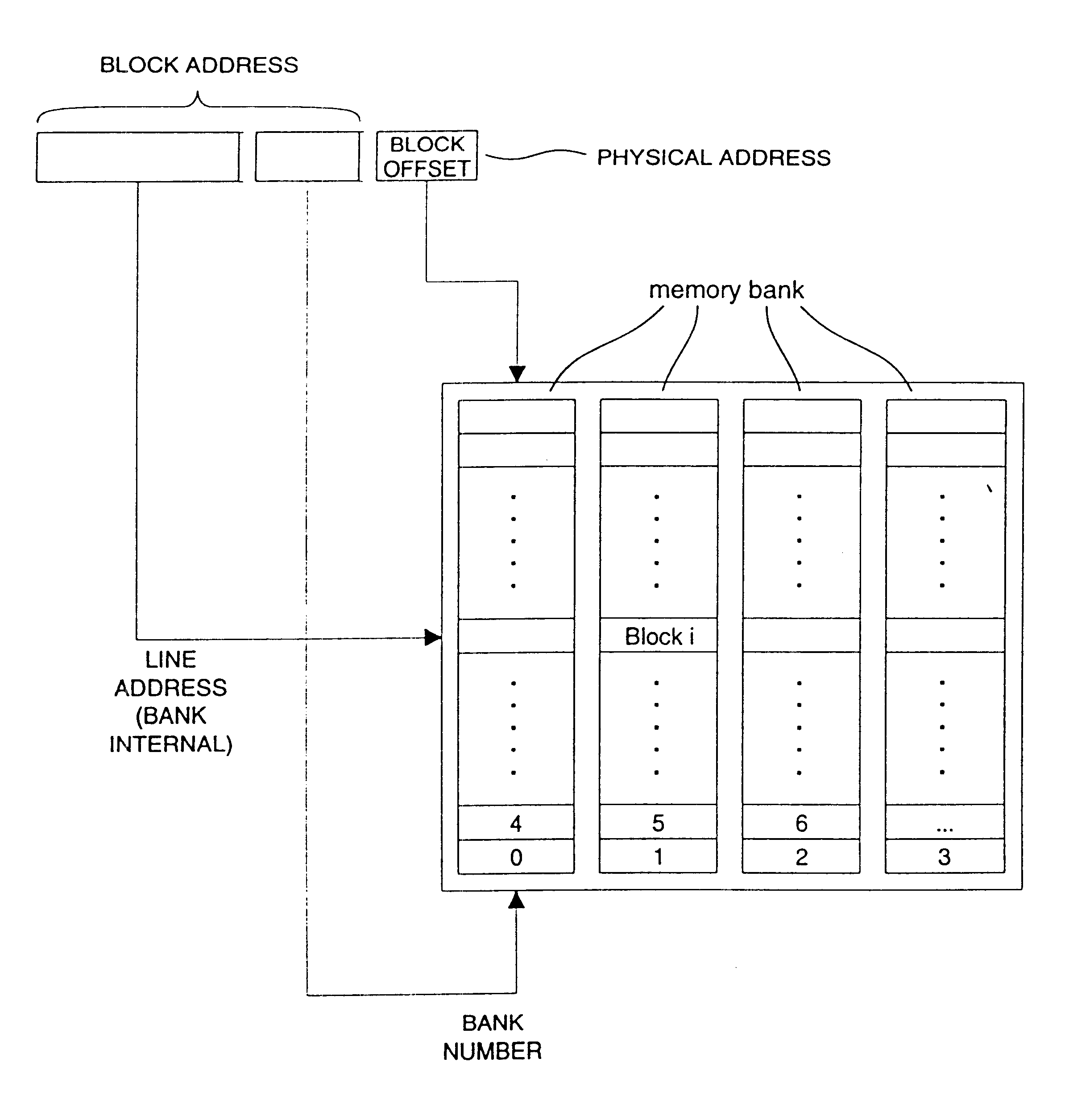
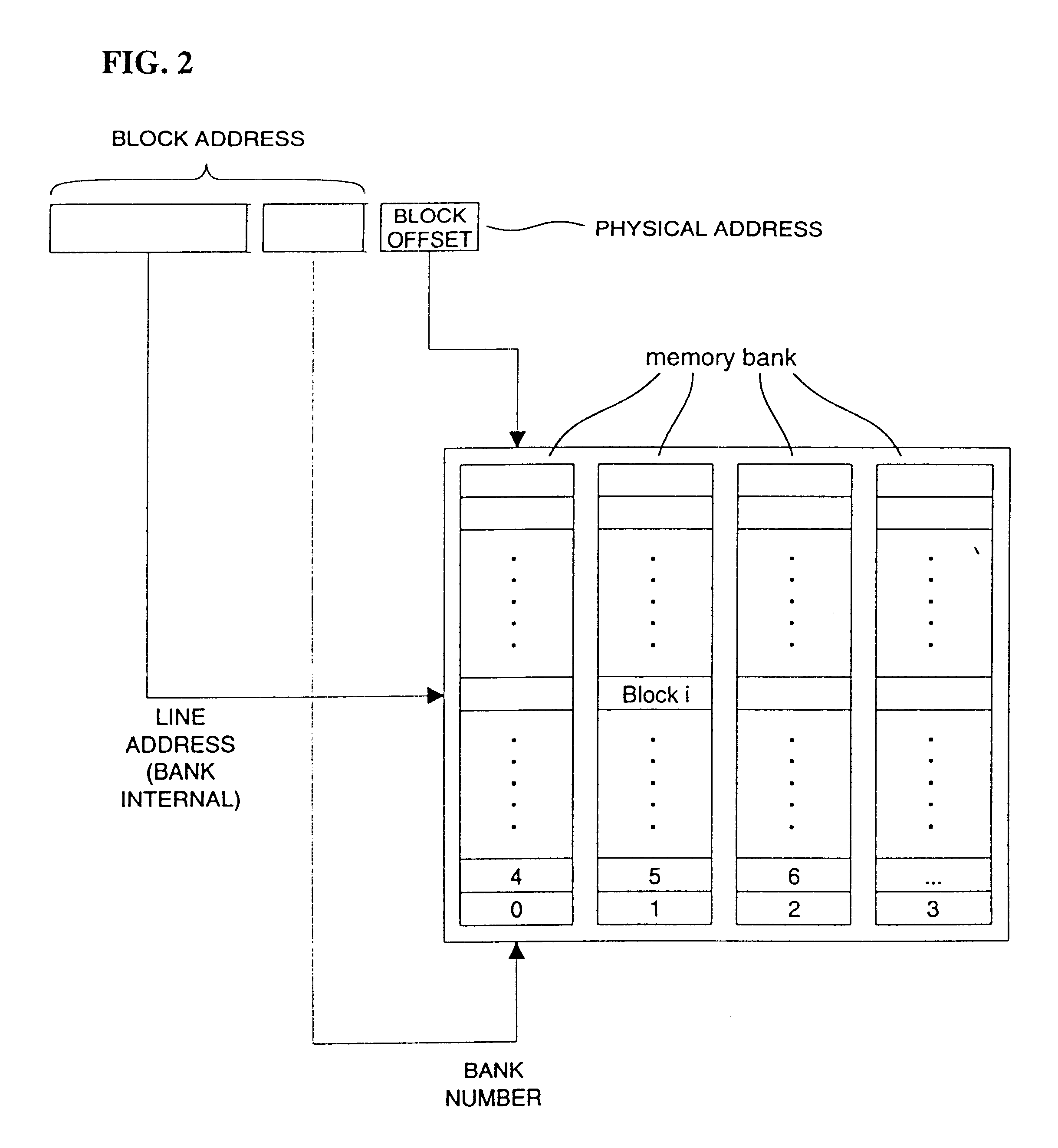
The bank number in which a given address is mapped, is obtained by performing a lookup operation using the X and Y portions taken from the address as index for the lookup table.

The least significant bit of the X portion is at bit position p.sub.0. Addresses that have a difference equal to 2.sup.p0 have the same Y value and consecutive X values. The column in the LUT corresponding to this Y value determines how addresses with consecutive X values are mapped over the memory banks and therefore, the interleave factor for an address sequence with a stride equal to 2.sup.p0.

In a similar way, addresses that have a difference equal to 2.sup.q0 have the same X value and consecutive Y values, where q.sub.0 is the bit position of the least significant bit of the Y portion. The row in the LUT corresponding to this X value determines how addresses with consecutive Y values are mapped over the memory banks, and therefore, the interleave factor for an address sequence with a str...


PUM


Abstract

For optimizing access to system memory having a plurality of memory banks, interleaving can be used when storing data so that data sequences are distributed over memory banks. The invention introduces an address-mapping method applying a table lookup procedure so that arbitrary, non-power-of-two interleave factors and numbers of memory banks are possible for various strides.

Description

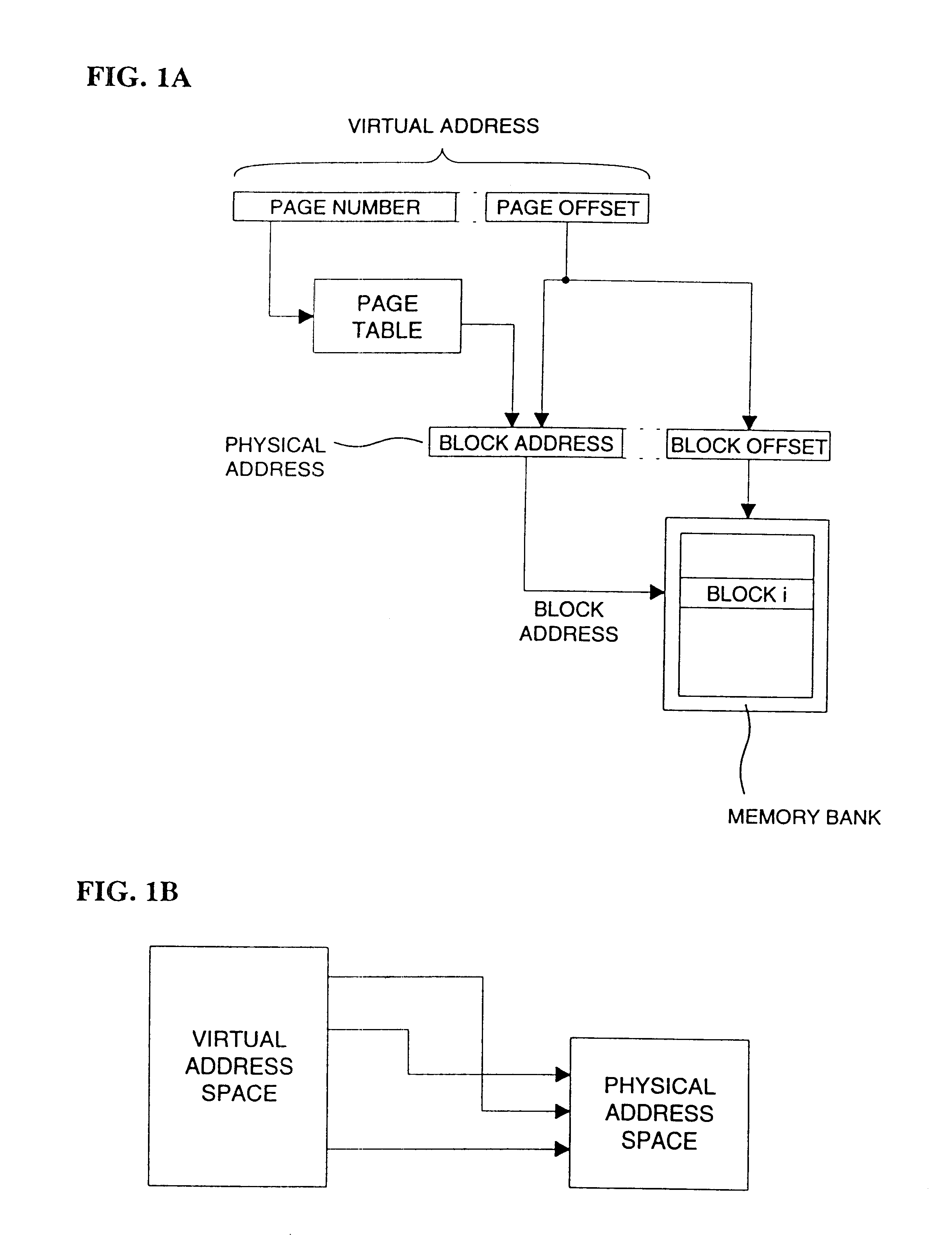
Present invention relates generally to address mapping for accessing system memory, and more particularly to address mapping for memories consisting of a plurality of memory banks in which interleaving of stored information is effected.Meaning of TermsAs some technical terms are not used uniformly in this field, a few definitions are given in the following to clarify the meaning of terms as they are used in this patent application.Virtual address=an address as used in programs (normal meaning)Physical address an address uniquely identifying the position in memory (as obtained from a virtual address e.g. by a table lookaside operation)Memory bank=a piece of memory that can be separately accessed (also called memory module; it may be a memory chip)Location=a storage place which can be separately addressed, can store usually one byte or wordLine=a portion of a memory bank handled as a whole and addressed as a whole, often consists of a power of 2 number of locations (1, 2, 4, etc.)Bloc...

Claims


Application Information

Patent Timeline
IPC IPC(8): G06F12/06
CPCG06F12/0607
Inventor LUNTEREN, JAN VAN
Owner TWITTER INC
Learn More