Double silicon-on-insulator device and method thereof

a silicon-on-insulator and double silicon technology, applied in the direction of semiconductor devices, semiconductor/solid-state device details, electrical apparatus, etc., can solve the problems of voltage limitations and cross-device interference, diodes, field effect transistors (fets) and bipolar transistors formed on silicon wafers are subject to parasitic effects, and discrete devices have limited applications

Inactive Publication Date: 2002-05-07
GLOBALFOUNDRIES INC
View PDF24 Cites 63 Cited by
  • Summary
  • Abstract
  • Description
  • Claims
  • Application Information

AI Technical Summary

Problems solved by technology

Typical prior art bulk silicon such as diodes, field effect transistors (FETs) and bipolar transistors formed on a silicon wafer are subject to parasitic effects resulting from other bulk devices in close proximity and from vertical structural asymmetry.
These parasitic effects include voltage limitations and cross-device interference.
However, these discrete devices have limited applications and do not have any of the advantages of monolithic circuit integration.

Method used


Image

  • Double silicon-on-insulator device and method thereof
  • Double silicon-on-insulator device and method thereof
  • Double silicon-on-insulator device and method thereof

Examples


Embodiment Construction

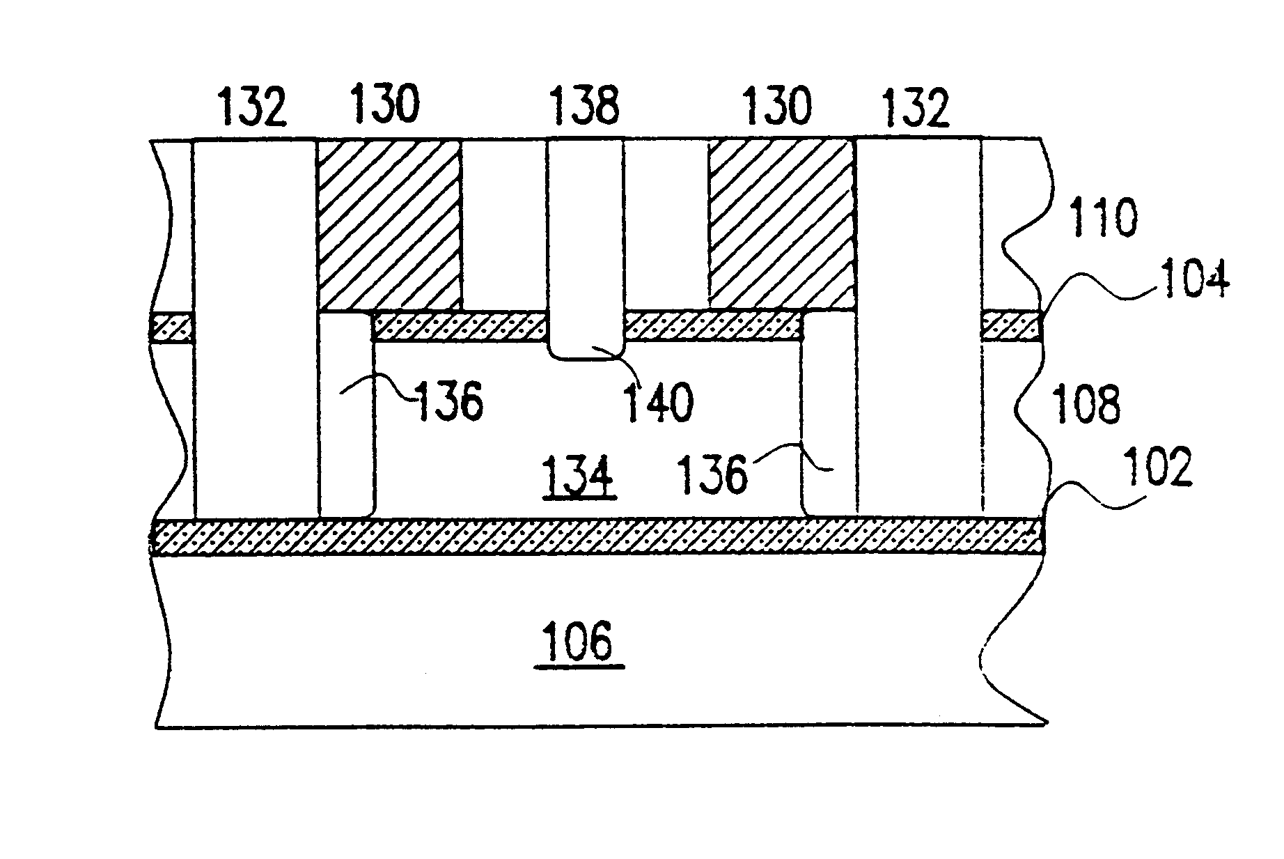
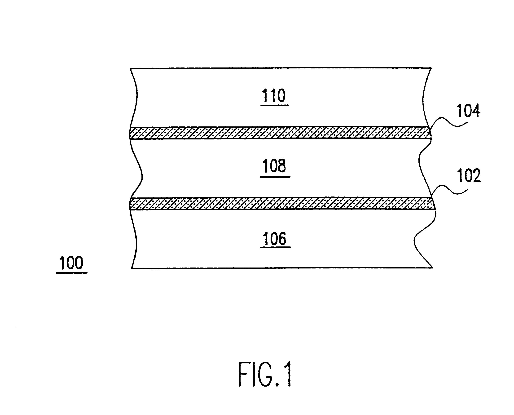
Referring now to the drawings, and more particularly to FIG. 1, the preferred embodiment structure is formed in a semiconductor wafer 100, preferably silicon, by implanting oxygen, which during a subsequent anneal reacts with the silicon to form buried oxide (SiO.sub.2) layers 102, 104. Thus, individual silicon layers 106, 108 and 110 are formed and isolated from each other by oxide layers 102, 104.

Although the structure of FIG. 1 is shown as including two buried oxide layers 102, 104 defining three individual silicon layers, any number of buried layers 102, 104 may be formed using multiple oxygen implants to formed a multi-layered structure, i.e., implanting n oxygen layers to define n+1 silicon layers, where n is a positive integer.

Further, although the preferred method of forming the multi-layer structure 100 of FIG. 1 is by implanting oxygen into silicon, the multi-layer structure 100 may be formed by any appropriate manner. So, for example, a single insulator (SiO.sub.2) layer ...


PUM


Abstract

An integrated circuit chip wherein one or more semiconductor devices are completely isolated from bulk effects of other semiconductor devices in the same circuit and a method of making the integrated circuit chip. The devices may be passive devices such as resistors, or active devices such as diodes, bipolar transistors or field effect transistors (FETs). A multi-layer semiconductor body is formed of, preferably silicon and silicon dioxide. A conducting region or channel is formed in one or more of the layers. For the FET, silicon above and below the channel region provides controllable gates with vertically symmetrical device characteristics. Buried insulator layers may be added to isolate the lower gate of individual devices from each other and to create multiple vertically stacked isolated devices. Both PFET and NFET devices can be made with independent doping profiles in both depletion and accumulation modes.

Description

1. Field of the InventionThe present invention generally relates to semiconductor devices and more particularly to silicon junction devices formed in silicon on insulator (SOI) technology.2. Background DescriptionTypical prior art bulk silicon such as diodes, field effect transistors (FETs) and bipolar transistors formed on a silicon wafer are subject to parasitic effects resulting from other bulk devices in close proximity and from vertical structural asymmetry. These parasitic effects include voltage limitations and cross-device interference.Consequently, typical bulk semiconductor processes, especially FET processes that include both p-type FETs (PFETs) and n-type FETS (NFETs) and commonly referred to as CMOS, require dedicated structures to localize and reduce parasitic effects. These specialized structures include providing surface diffusions referred to as guard rings, individual doped wells (N-wells and / or P-wells) and including a buried insulator.Discrete devices, i.e., indi...

Claims


Application Information

Patent Timeline
Patent Type & Authority Patents(United States)
IPC IPC(8): H01L21/70H01L21/762H01L21/02H01L29/73H01L21/265H01L21/329H01L21/331H01L27/085H01L27/12H01L29/786
CPCH01L21/7624H01L27/085
Inventor COLT, JR., JOHN Z.
Owner GLOBALFOUNDRIES INC
Why Eureka
Try Eureka