Developing process and developing unit

a technology of developing unit and developing process, which is applied in the direction of photosensitive material processing, instruments, photosensitive materials, etc., can solve the problems of deterioration, shortening the time required to switch the operation, and affecting the operation

Inactive Publication Date: 2002-07-16
TOKYO ELECTRON LTD
View PDF5 Cites 34 Cited by
  • Summary
  • Abstract
  • Description
  • Claims
  • Application Information

AI Technical Summary

Problems solved by technology

Consequently, since the front surface of the wafer is unequally developed, the line width of the circuit pattern may deviate to some extent.
In addition, as described above, since a high resolution circuit pattern has been required, a slight deviation of the line width may cause the yield to deteriorate.
Thus, it takes...

Method used


Image

  • Developing process and developing unit
  • Developing process and developing unit
  • Developing process and developing unit

Examples


Embodiment Construction

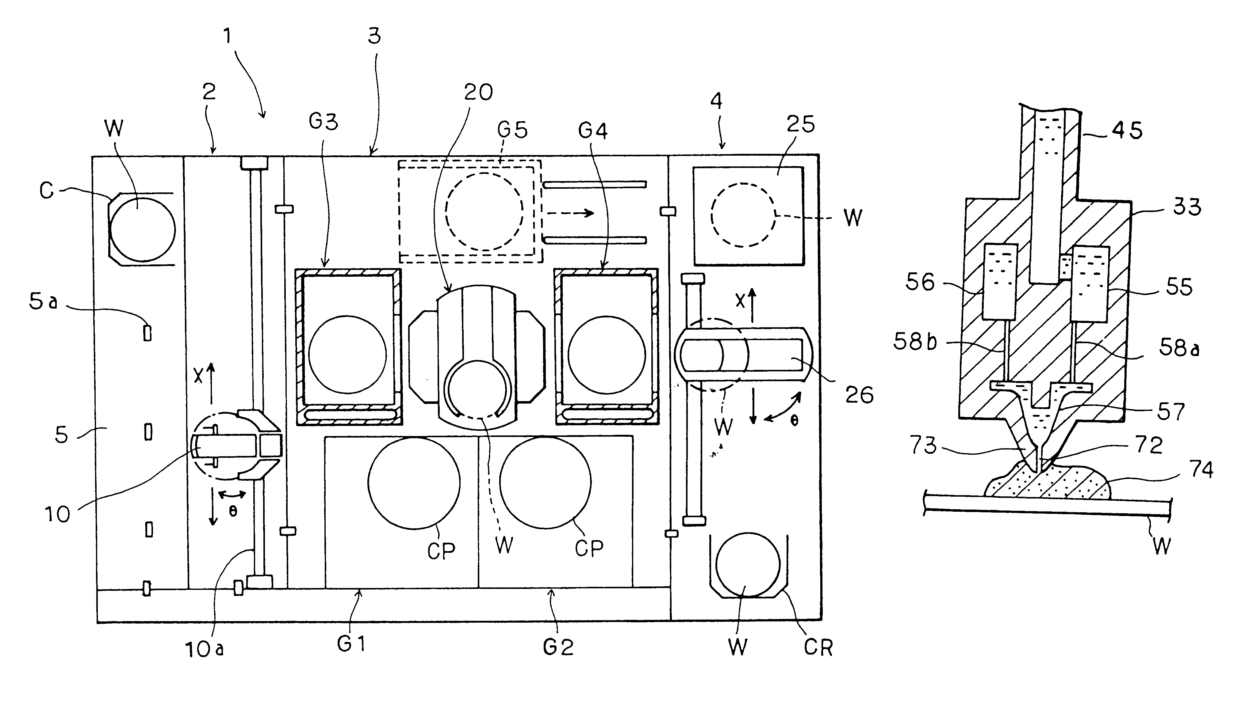
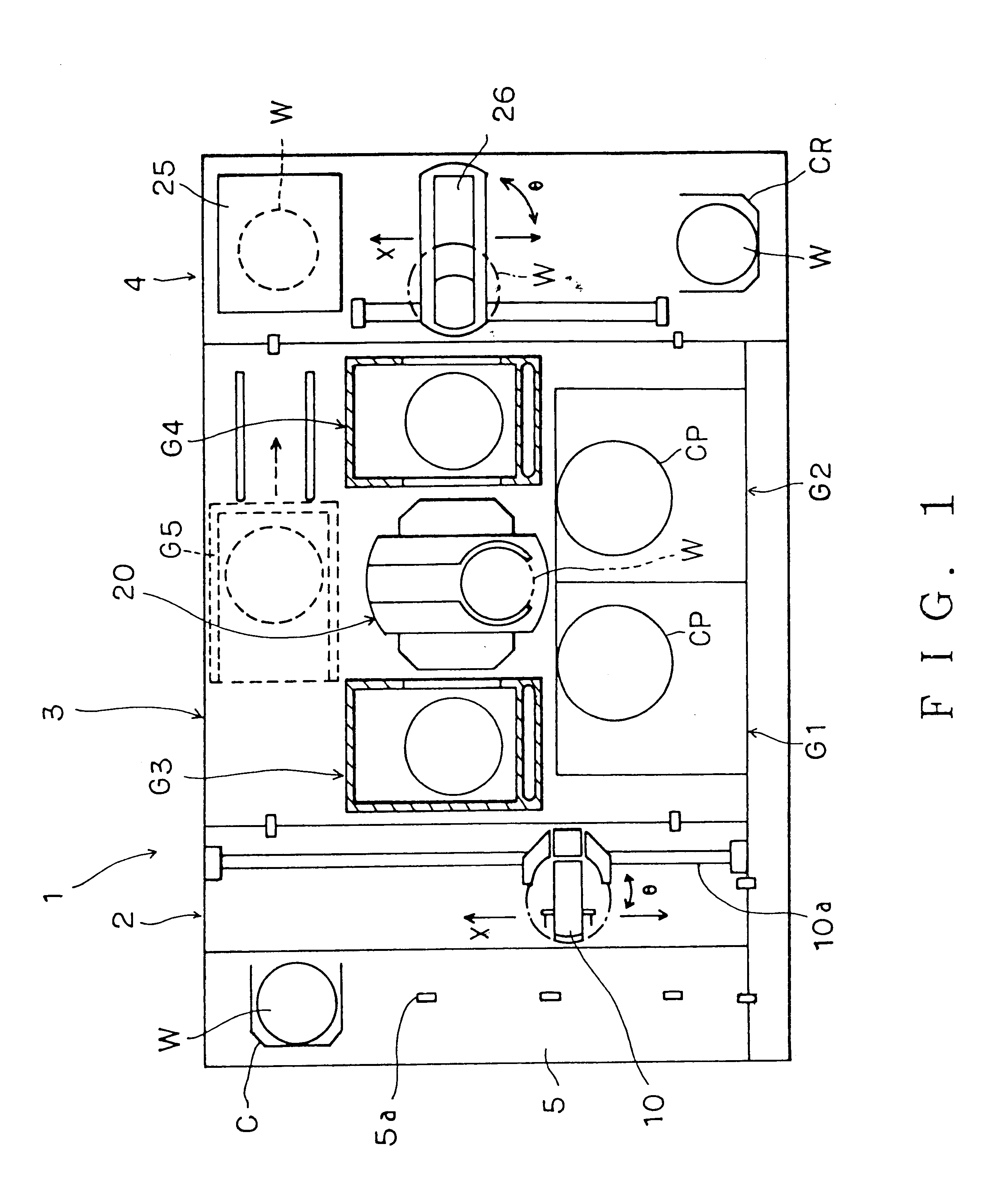
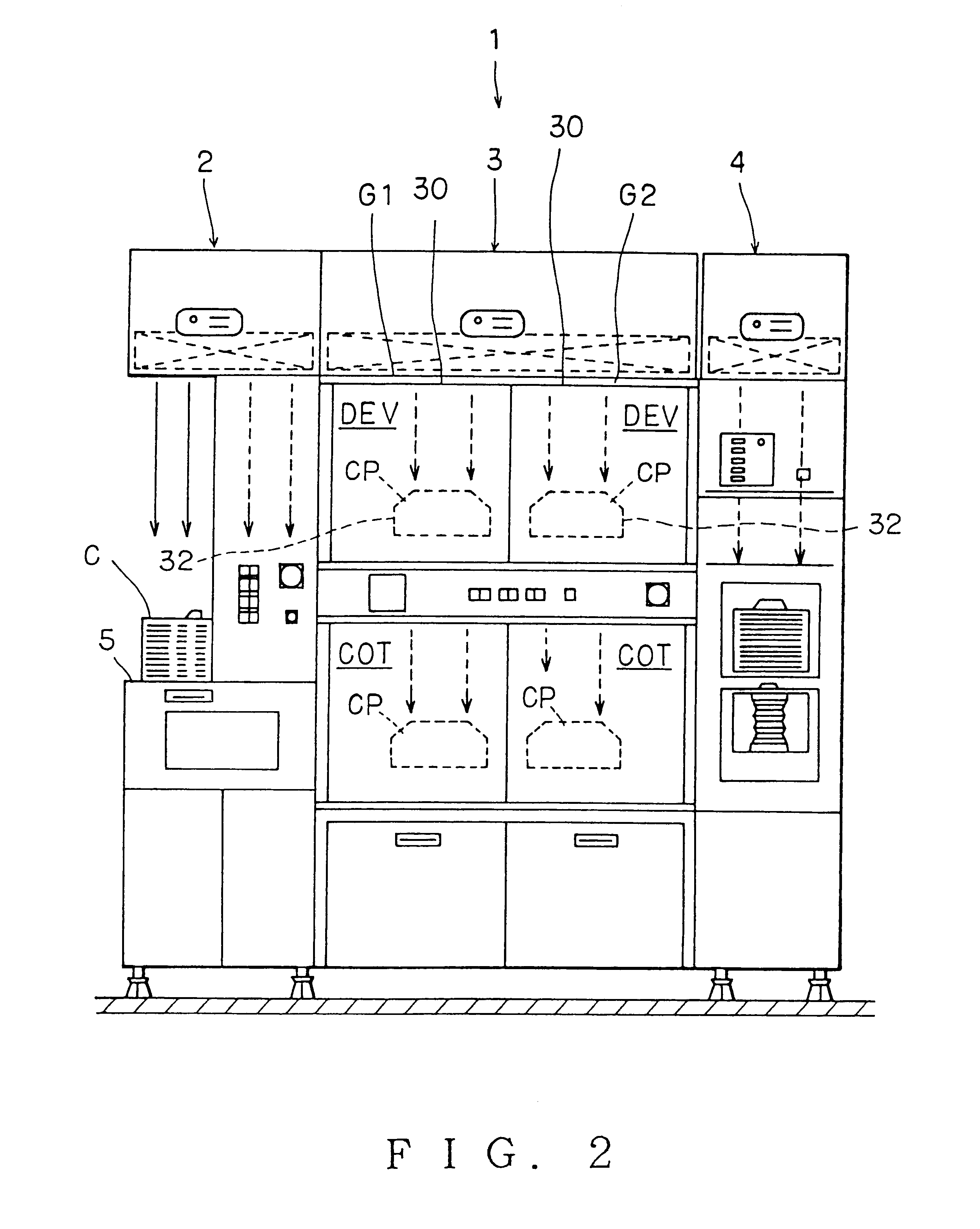
FIG. 1 shows the structure of a coating and developing system 1. The coating and developing system 1 comprises a cassette station 2, a processing station 3, and an interface portion 4 that are integrally disposed and connected. The cassette station 2 loads and unloads a cassette C containing for example 25 wafers W to / from the coating and developing system 1. In addition, the cassette station 2 loads and unloads a wafer W to / from the cassette C. The processing station 3 has various processing units arranged in a plurality of stages. Each of the processing units performs a particular process for each wafer W. The interface portion 4 transfers a wafer W between the processing station 3 and an exposing unit (not shown) disposed adjacent thereto.

The cassette station 2 has a plurality of cassettes C at alignment protrusions 5a on a cassette holding table 5 in such a manner that the cassettes C are arranged in X direction (the upper and lower directions of the drawing shown in FIG. 1) and...


PUM


Abstract

When a developing process is performed, a mixture of developing solution and pure water is supplied while the ratio of developing solution and pure water is gradually increased from pure water to developing solution. Thus, a developing solution component and a resist component gradually react. Even if a resist component dissolves in the mixture of pure water and developing solution, the equality of the concentration of the developing solution can be maintained. Thus, the developing process can be suppressed from being unequally performed. When a rinsing process is performed, a mixture of developing solution and pure water is supplied while the ratio of developing solution against pure water is gradually decreased from developing solution to pure water. Consequently, the substitution from developing solution to pure water can be gradually performed. As a result, particles due to the solidification of unsolved resist can be prevented.

Description

1. Field of the InventionThe present invention relates to a developing process and a developing unit for supplying developing solution to the front surface of a substrate such as a semiconductor wafer or an LCD substrate.2. Description of the Related ArtIn a resist process of a semiconductor fabrication, resist solution is coated as a resist film on the front surface of a substrate such as a semiconductor wafer (referred to as wafer). A predetermined pattern is formed on the front surface of the wafer by an exposing unit. Developing solution is coated to the front surface of the wafer. Thereafter, a rinsing process for rinsing the developing solution with pure water is performed.Developing solution is supplied as a liquid layer to the front surface of the wafer. In this state, the developing process is performed for a predetermined time period. In the developing process, a positive photoresist of which an exposed portion is dissolved with developing solution has been widely used bec...

Claims


Application Information

Patent Timeline
IPC IPC(8): G03D5/00G03D5/04H01L21/027G03F7/30
CPCG03D5/04
Inventor INADA, HIROICHI
Owner TOKYO ELECTRON LTD
Why Eureka
Try Eureka